Gold standard for JEDEC® ONFI memory device for your IP, SoC, and system-level design verification.

In production since 2011 for dozens of production designs.

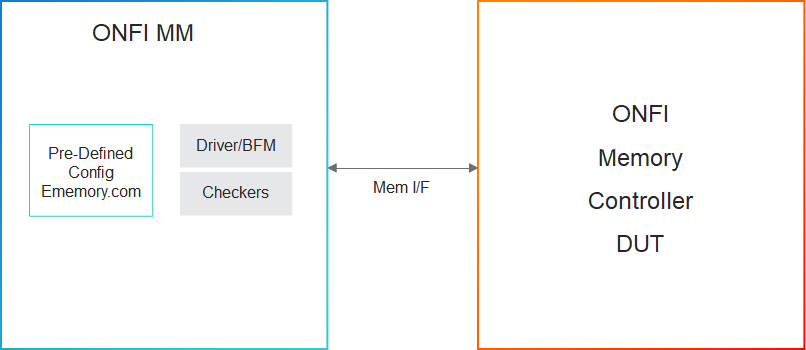
The Cadence® Memory Model Verification IP (VIP) for ONFi is the verification solution for NAND flash memory interface based on any version of the Open NAND Flash interface. The VIP supports all the interfaces: SDR, NV-DDR, NV-DDR2, NV-DDR3, and NV-LPDDR4, as defined in the standard. The interface mode can be dynamically switched from one to another during the simulation till NV-DDR2. Through the "Volume Address" feature, defined in the latest standard, any number of device models can be connected to a single "chip enable" signal to allow testing of CE_n pin reduction scenarios.

Supported specification: JEDEC ONFi versions 1.0, 2.0, 3.0, 4.0, 4.1, 4.2, 5.0, 5.1

ONFI diagram

Product Highlights

  • Hundreds of protocol and timing checkers to easily catch design bugs
  • Hundreds of predefined configurations based on specific memory vendors' part numbers, datasheets, or generic JEDEC definitions available on ememory.com
  • Transaction and memory callbacks for all protocol, model states and device memory events
  • Error injection capability through user modification of transaction contents
  • Ability to check for errors and change error severity
  • Ability to dynamically change configuration parameters
  • Packet tracker creation for easy debugging
  • Support testbench language interfaces for SystemVerilog and UVM

Key Features

The following table describes key features from the specifications that are implemented in the VIP:

Feature Name

Description

Speed

  • NV-DDR3: 800MHz, 1600MT/s (DDR)
  • NV-LPDDR4: 1200MHz, 2400MT/s (DDR)

Interfaces

  • SDR, NV-DDR, NV-DDR2, NV-DDR3, and NV-LPDDR4. With ability to switch among interface modes dynamically. Available on low-voltage operation of the device to provide faster throughput and improved I/O Power consumption

General Functionality

  • Reset, Read Device ID parameters, Read status of NAND device and LUNs, Multi-plane Read, Cache Read, Program, Erase, and Copyback operations, Multi-LUN operations, LUN Get/Set commands, ZQ Calibration, Set/Get Feature addresses.

Core and Bus timing

  • Setup/Hold, Per Lane or Per Bit, Pulse width

Timing Modes

  • Timing Modes Up to Timing Mode 22

Training

  • Explicit and Implicit DCC Training, Read DQ training, Write DQ Training at TX side

CE_n Pin Reduction

  • Allows multiple devices, model instances, to be connected to a single "chip enable"

Data Eye

  • User configurable timing parameters to corrupt data eye during read path

ONFI 5.0 Features

  • ODT Disable and Enable commands, DBI

ONFI 5.1 Features

  • Differential Signaling on power up
  • Trainings: Per-pin VrefQ Adjustment
  • Supported parameters page for new trainings and timing modes
  • New feature addresses for WDCA and Per-Pin VrefQ Training

Master Your Tools

Tutorials, Documentation, and Local Experts

Cadence Online Support

Increase your efficiency in using Cadence Verification IP with online trainings, VIP Portal, application notes, and troubleshooting articles