Gold standard for Hyperflash memory device for your IP, SoC, and system-level design verification.

Hyperflash in production since 2018 for many production designs.

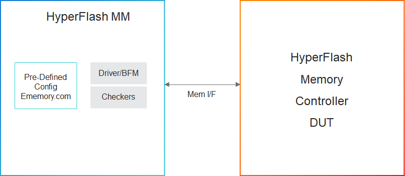
The Cadence® Memory Model Verification IP (VIP) for HyperFlash provides verification of HyperFlash Controller using the HyperBus protocol. It provides a mature, highly capable compliance verification solution applicable to intellectual property (IP), system-on-chip (SoC), and system-level verification. The VIP for HyperFlash is compatible with the industry-standard Universal Verification Methodology (UVM), runs on all leading simulators, and leverages the industry-standard Cadence Memory Model core architecture, interface, and use model.

Supported specification: Features of Cypress specification Document Number: 001-99198 Rev. *H Revised February 06, 2017.

HyperFlash diagram

Product Highlights

  • Hundreds of protocol and timing checkers to easily catch design bugs
  • Dozens of predefined configurations based on specific memory vendors' part numbers, datasheets, or generic definitions available on ememory.com
  • Transaction and memory callbacks for all protocol, model states, and device memory events
  • Error injection capability through user modification of transaction contents
  • Ability to dynamically change configuration parameters
  • Ability to check for errors and change error severity
  • Packet tracker creation for easy debugging
  • Support testbench language interfaces for SystemVerilog and UVM

Key Features

The following table describes key features from the specifications that are implemented in the VIP:

Feature Name

Description

Density

  • From 128Mb to 512Mb

General Functionality

  • Supports Status Register Read and Clear commands
  • Supports Program, Read commands for POR Timer Register
  • Supports Interrupt Control and Status Registers
  • Supports Volatile and Non-Volatile Configuration Control Registers
  • Read memory array data, Program data into memory, Program data to flash memory
  • Supports commands for Erase, Suspend and Resume, Blank check, Enter Deep Power Down
  • Support Program buffer to flash confirm command
  • Support Device Input and Output timing and Variants memory operations timing

Burst

  • Wrapped burst: Supports burst lengths: 16 bytes (8 clocks), 32 bytes (16 clocks), 64 bytes (32 clocks), linear burst and hybrid burst: One wrapped burst followed by linear burst

Reset Output Pin Functionality

  • Supports Reset functionality through: Hardware Reset (via RESET# pin), Reset and Address Space Overlay (ASO) Exit (0xF0) command, System-level power-on reset via RSTO#

Interrupt

  • Supports INT# output to generate external interrupt during: Busy to Ready Transition and ECC detection

DDR Center Aligned Read Strobe

  • Supports phase shifting of the RWDS signal with respect to the read data outputs using Phase Shifted Clock input PSC and PSC# pins

ASO Capability

  • Command support for for various ASOs such as: ID-CFI, ASPR ASO, Password ASO, PPB ASO, PPB Lock Bit ASO and DYB ASO

ECC

  • ECC Status Enter, ECC Status Read, Error Lower Address Register, Error Upper Address Register, Read Error Detection Counter and Clear ECC Errors

CRC

  • CRC ASO Entry, Load CRC Start/End Address, CRC Suspend, Array Read, CRC Resume, Read Check-Value Low/High Result Register

Master Your Tools

Tutorials, Documentation, and Local Experts

Cadence Online Support

Increase your efficiency in using Cadence Verification IP with online trainings, VIP Portal, application notes, and troubleshooting articles