Gold standard for Flash Toggle NAND memory device for your IP, SoC, and system-level design verification.

In production since 2011 for many production designs.

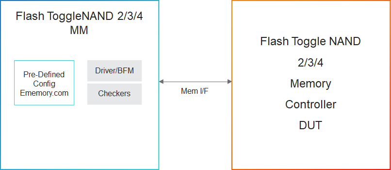
Cadence® Verification IP (VIP) for Toggle NAND is applicable to intellectual property (IP), system-on-chip (SoC), and system-level verification to provide verification of Flash NAND devices using toggle mode DDR 2.0 and above. The VIP for Toggle NAND is compatible with the industry-standard Universal Verification Methodology (UVM), runs on all leading simulators, and leverages the industry-standard Cadence Memory Model core architecture, interface, and use model.

Supported specification: toggle NAND DDR 2.0 Single-Level-Cell (SLC) and Multi-Level-Cell (MLC) devices as well as Toggle NAND DDR 3.0/4.0 Single-Level-Cell (SLC), Multi-Level-Cell, and Triple-Level-Cell (TLC) devices from Hynix, Samsung, Toshiba, and SanDisk.

Toggle NAND diagram

Product Highlights

  • Hundreds of protocol and timing checkers to easily catch design bugs
  • Hundreds of predefined configurations based on specific memory vendors' part numbers, datasheets, or generic JEDEC definitions available on ememory.com
  • Transaction and memory callbacks for all protocol, model states, and device memory events
  • Error injection capability through user modification of transaction contents (Below Version 2.0)
  • Packet tracker creation for easy debugging (Below Version 2.0)
  • Support testbench language interfaces for SystemVerilog, UVM
  • Ability to dynamically change configuration parameters

Key Features

The following table describes key features from the specifications that are implemented in the VIP:

Feature Name

Description

Speed

  • Up to 200MHz or 400Mbps per DQ pin
  • Up to 600MHz or 1200Mbps per DQ pin (Version 3.0/4.0)

Bits per Cell

  • Single-Level-Cell (SLC – 1-bit per cell) and Multi-Level-Cell (MLC – 2-bits per cell) devices support
  • SLC, MLC and Triple-Level-Cell (TLC – 3-bits per cell) devices support (Version 3.0/4.0)
Memory Sizes
  • 64Gb, 128Gb, 256Gb, and 512Gb

Configurability

  • Page size in number of bytes
  • Number of pages per block
  • Number of blocks per Plane/LUN (die/stack)
  • Number of Planes/LUNs per target
  • Number of targets per device

Commands

  • Software Reset
  • Read ID
  • Read Status
  • Read LUN status
  • ODT turn on and off

Operations

  • Multi-Plane and Interleaved operations for Read, Cache Read, Program, and Erase Operation
  • Multi-LUN Operations for simultaneous Read, Program, and Erase operations

Multiple Die

  • Supports Multiple Die with shared Chip Select signal

Signals

  • Differential signals support for Data Strobe Signal and Read Enable Signal

LUN Features

  • Supports LUN Set and Get Features to set NAND device in certain modes

Simulation Test Suite

MM has a rich test suite of scenarios for easy MM evaluation and deployment.

Please contact us for further information.

Master Your Tools

Tutorials, Documentation, and Local Experts

Cadence Online Support

Increase your efficiency in using Cadence Verification IP with online trainings, VIP Portal, application notes, and troubleshooting articles