Gold standard for JEDEC® LPDDR5 memory device for your IP, SoC, and system-level design verification.
In production since 2015 on dozens of production designs.
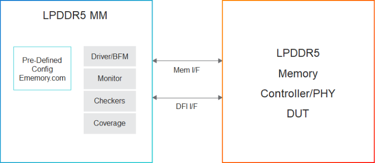
This Cadence® Verification IP (VIP) supports the JEDEC® Low-Power Memory Device, LPDDR5 standard. It provides a mature, highly capable compliance verification solution that supports simulation, formal analysis, and hardware acceleration platforms, making it applicable to intellectual property (IP), system-on-chip (SoC), and system-level verification. The VIP for LPDDR5 is compatible with the industry-standard Universal Verification Methodology (UVM), runs on all leading simulators, and leverages the industry-standard Cadence Memory Model core architecture, interface, and use model.
The LPDDR5 standard is an industry-leading low-power volatile (DRAM) device memory standard for storage of system code, software applications, and user data. The LPDDR5 Low-Power Memory Device Standard is designed to satisfy the performance and memory density demands of the latest generation of mobile devices such as smartphones, tablets, ultra-thin notebooks, and similar connected devices on the newest, high-speed 4G networks.
Supported specification: The VIP for LPDDR5 Memory Model supports the latest proposals which are balloted at JEDEC for LPDDR5 and LPDDR5x and the specifications: JESD209-5A and JC-42.6-1854.99A dated 2019/10/04.
Product Highlights
Hundreds of protocol and timing checkers to easily catch design bugs
Hundreds of predefined configurations based on specific memory vendors part numbers datasheets or generic JEDEC definitions available on ememory.com
Transaction and memory callbacks for all protocol, model states and device memory events
Ability to optionally skip initializations or dynamically change configuration parameters
Packet tracker creation for easy debugging
Extensive functional coverage in SystemVerilog
Integrated with the DFI LPDDR5 solution for IP level verification
Plug-and-play connectivity to System Performance Analyzer for Sub-system or SoC performance verification
Support testbench language interfaces for SystemVerilog, UVM, OVM and SystemC
Key Features
The following table describes key features from the specifications that are implemented in the VIP:
Feature Name
Description
Speed
1066.5MHz (8533 Mbps)
Device Density
Supports a wide range of device densities from 2Gb to 32Gb
Bank Architecture
8B, 16B, and 4BankGroup
General DDR Functionality
Activation, Precharge, and Mode Register Write and Read, CAS, Mask Write, Read, Write, Mask Write, Power Down, Refresh, Self Refresh, and DSM command and related timing checks
Initialization Sequence
Bus timing: Setup/Hold Per Lane or Per Bit, Pulse width
Clock frequency change and clock stop and related checkers.
RDQS timing support
VREF Current Generator (VRCG)
Differential Clock (CK, WCK) checks
Duty Cycle Monitor (DCM)
Temperature Derating
tHZDQ, tHZDQS
Core timing table when Link ECC is enabled
User configurable timing parameters to corrupt data eye during read path
Training Modes
Enhanced RDQS training mode
Read DQ Calibration
Write Leveling
Command Bus Training Mode1 and Mode2
WCK2DQoscillator
RDQS toggle mode
Read FIFO and Write FIFO
Link ECC WCK-RDQS_t/Parity Training using FIFO
Vref CA and DQ training
Read/Write based WCK-RDQS_t Training
Write Clock
WCK2Ck synchronization
4:1 and 2:1 WCK to CK ratio
WCK Sync off timing
WCK2DQ AC timings for low and high frequency
Enhanced WCK always On
Write clock-related timing parameter support - tWCH, tWCL, tWCK(avg), and tJIT
WCK suspend mode - tWCKSUS
Low Power Consumption Features
Read and Write Datacopy
Write-X
WXS, WXSA, and WXSB support (byte controllable writex)
Configurable Preamble and Postamble
Allows preamble and postamble to be configured for Read, Write, and Mask Write
Data Bus Inversion
Data on the bus can be inverted during both read and write to save power
Frequency Set Points
Allows LPDDR5 to be switched between three different operating frequencies by duplicating mode register parameters commonly changed with operating frequency
Exploration Mode
VIP acts as a passive monitor without driving data and only checks for the command protocols: Read, MRR, Write, and Mask Write
MPC
Supports all 6 MPC commands
Command Bus Training
The training centers the internal VREF(ca) in the CA data eye and, at the same time, allows timing adjustments of the CS and CA signals to meet setup and hold requirements
Latency Code Frequency Table
Checks all read and write latency requirements for a given frequency
Tccd+n Reads and Writes
All combinations of Reads merging and Writes merging placed Tccd+n apart
Delay Modeling
Delay modeling of input and output signals, display of delay modeling internal signals on the simulator waveform
Single-Ended Clock
Single-Ended Clock, Write Clock, and RDQS support
Byte Mode
Support for Byte Mode (x8) devices
Refresh
Refresh rates and options to control the application of new rates
Temperature Derating
Support for temperature derating and per-timing derating factor
Link-ECC
Support for Write and Read Link Error Correcting Code
DMI Pin Behavior
DMI Pin behavior based on Read/Write-related commands
ODT
Support for On Die Termination on timings, which is command-to-command timing checks with ODT enabled, tODTup, tDQ7FSP
ZQ Calibration
Support for command based and background ZQ calibration
Skew Support
Support for adding skew on RDQS using tDQSQ
Support for adding skew on bytelane during Write using tWCKDQISkew
Duty Cycle Adjuster
Support for controlling the duty cycle of RDQS/DQ during Reads
RDQS Glitch Modeling
Ability to add glitches on RDQS
Rank to Rank Timing Checks
Support for rank2rank timing checks using LPDDR5MDP
Support includes all the Rank-to-Rank timing constraints available in JESD209-5A spec
Refresh Management
Support for Refresh Management functionality
Monitor Mode
In this mode, the DRAM will perform complete protocol validation. However, the DRAM will not drive (output) any data on I/O pins.
DFE
Support for Decision Feedback Equalization includes: Rank to rank timing constraints affected with enabling DFE and tDPRE pre-drive requirement before the write data burst operation
Functional Coverage
Provides a rich functional coverage of the model
Inter-rank timing checks coverage is provided withLPDDR5MDP
Delay Randomization
Support for delay randomization on WCKDQO with drifts