Best-in-class DFI™ Verification IP for your IP, SoC, and system-level design testing.
Complete solution for extensive and fast verification used by multiple production designs.
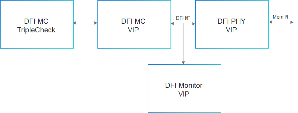
The Cadence Verification IP (VIP) for DFI provides a mature, highly capable compliance verification solution for the DFI protocol. The VIP supports the simulation platform and enables metric-driven verification of IP and system-on-chip (SoC) designs against DFI protocol specifications. DFI VIP supports both the memory controller (MC) traffic generation and the PHY component, which samples from the DFI interface and drives to the memory interface for different memory variants. The VIP for DFI is compatible with the industry-standard Universal Verification Methodology (UVM) and supports all leading simulators.
Supported specification: DDR PHY Interface Specification v4.0, v5.0 and v5.1
Product Highlights
Generates constrained-random bus traffic with predefined error injection
Hundreds of protocol and timing checkers to easily catch design bugs
Callbacks access at multiple TX and RX queue points for scoreboarding and data manipulation
Ability to optionally skip initializations or dynamically change configuration parameters
Dynamic activation support to enable the user to set the VIP as active or passive without changing the testbench while determining which instance to instantiate during run time
Packet tracker creation for easy debugging
Extensive functional coverage in SystemVerilog
Integrated with the DRAM Memory Models for complete IP-level verification
MM-DFI Auto Config - Automatic updates of timing parameters of DFIMC/DFIPHY VIP based on MM configuration
Support testbench language interfaces for SystemVerilog, UVM, OVM, e, and SystemC
Key Features
The following table describes key features from the specifications for the simulated DFI MC and DFI PHY that are implemented in the VIP:
Feature Name
Description
Supported Memory
DFI MC
Command Interface
Drives Command on different phases based on memory protocol requirement
DDR4-5, LPDDR4-5, HBM2E-3 and GDDR6-7
Command-to-Command Delay
Configurable different timing constraint requirements while driving a command through DFI interface for the memory
DDR4-5, LPDDR4-5, and HBM2E-3
Data Interface
Read and Write Data Interface
DDR4-5, LPDDR4-5, HBM2E-3 and GDDR6-7
Update Interface
MC-initiated and PHY initiated updates
DDR4-5, LPDDR4-5, HBM2E-3 and GDDR6-7
Training Interface
CA, Write, Write DQ, Read Training (Both MC initiated and PHY initiated)
DDR4, LPDDR4
PHY Master Interface
Supports PHY Master Interface
DDR4-5, LPDDR4-5, HBM2E-3 and GDDR6-7
WCK Interface
Supports WCK Interface
LPDDR5
Frequency Change Protocol
Initiates frequency change
DDR4-5, LPDDR4-5, and HBM2E-3
Low-Power Control
Initiates Low-Power Entry as per DFI5.0 and DFI4.0
DDR4-5, LPDDR4-5, HBM2E-3 and GDDR6-7
Data CS Gap
Data Path Chip Select Gap (per Rank Delay line support)
DDR4-5, LPDDR4-5, and HBM2E-3
Refresh Command
Sends Refresh All and Refresh Per Bank command on every internal
DDR4-5, LPDDR4-5, and HBM2E-3
DFI Interactions
DFI Interaction Rules as per DFI 5.0
DDR5, LPDDR5, HBM3, GDDR6-7
2N Mode
Command transmission in 2N Mode
DDR5
DBI and Data Mask
Generates Inverted/Masked Write Data and Invert received Read Data with dfi_rddata_dbi enabled
DDR4-5, LPDDR4-5, and HBM2E-3
CRC
Generates CRC and error injection
DDR4-5
Frequency Ratio
All possible frequency ratios as per specification
DDR4-5, LPDDR4-5, HBM2E-3 and GDDR6-7
GearDown Mode
Command transmission in GearDown Mode
DDR4
Checkers
Performs timing and protocol checks for signals driven by PHY