Overview
The Best Analog Design Solution Just Got Better
Cadence Virtuoso Studio, an application of the Cadence.AI Generative AI Platform, leverages 30 years of industry knowledge and leadership in custom/analog design to give you broader support for systems, including RF, mixed-signal, photonics, and advanced heterogeneous designs. Innovative artificial intelligence (AI) techniques, cloud enablement, infrastructure improvements, and integration across Cadence products complement these design flows, creating a hub for efficiently delivering real designs for the real world.

Key Benefits
Analog Design Reimagined for Productivity and Interoperability
The Virtuoso Studio custom design solution provides innovative features, reimagined infrastructure for unrivaled productivity, and new levels of integration that stretch beyond classic design boundaries.
Integrated Solutions
Support for entire flow from chip design to advanced packaging creation to board layout
Infrastructure Productivity
Comprehensive planar and FinFET-based automation providing better throughput and productivity
Cloud Ready
Massively scalable, cloud-ready solutions for when 100s of simulations turn into 1,000s
Innovative Generative AI Usage
AI-enabled tools learn and improve next-generation designs
Heterogenous Integration
Allows heterogenous integration of 2.5D or 3D designs for RF and photonics systems
Highlights
Comprehensive, Integrated Solutions Provide the Foundation for Virtuoso Studio
Custom IC
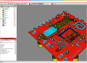
Cadence custom integrated circuits (ICs) design solutions offer an ideal balance of automation and custom-crafting, including managing design intent that flows naturally from the schematic throughout all phases of the design. The extensive analysis environment facilitates real-time knowledge of circuit status compared to specifications, with both pre-and post-layout parasitics considered. The layout tools are designed with productivity features to facilitate connectivity right designs regardless of rule complexity. Integrated verification methods, both in the front-end and back-end spaces, provide real-time knowledge of design progress, given all the interdependencies commonly impacting circuit performance in analog, RF, and mixed-signal design.
Advanced Node
Advanced-node processes challenge custom/analog designers with the complex interdependency of manufacturing and variability, on top of increasing power and performance specifications. The Cadence Virtuoso advanced-node platform has innovative capabilities that enable designers to take full advantage of the silicon at these process nodes.
The Virtuoso advanced-node platform improves individual point tools to handle these challenges while enabling new design methodologies that allow rapid layout prototyping, in-design signoff, and close collaboration between schematic and layout designers—essential to designing efficiently at advanced-process nodes.
Heterogeneous Design
Combining different types of semiconductors into a single system allows size and power reduction while providing higher-performance RF, photonics, and wired interfaces. Integrating chiplets helps implement circuits with individual but optimal processes, leading to overall cost reduction and faster time-to-market. Numerous advances in Virtuoso Studio allow designers to meet heterogeneous design challenges such as multi-fabric co-analysis of electrical, electromagnetic, and photonic signals, as system-level integration and verification, including power and thermal analysis.
Migration
Virtuoso Studio pioneers the next era of migration tools for custom IC design. The migration of designs across process nodes has evolved over many tool generations. To assist their advanced-node customers, the world’s foundries have teamed up with Cadence to produce new techniques in moving schematic and layouts efficiently to new nodes and using updated analysis tools to ensure optimal results.;
Photonics
Built upon the Virtuoso Studio, the electronic/photonic design automation (EPDA) environment supports monolithic (single chip with both electronic and photonic components) and hybrid (3D-IC stacks with a traditional electronics IC on top of a photonics IC) approaches. The comprehensive EPDA flow provides schematic capture, circuit simulation, and schematic-driven layout implementation, as well as support for complex photonic SKILL PCells and advanced photonic layout generators. It also includes co-design of the electronic and photonic components for hybrid systems.
RF Design
The demand for more sophisticated wireless connected devices is driving the need for a new generation of high-performance, cost-sensitive silicon products, often implemented in highly integrated, multi-device, and multi-fabric modules.
Cadence Virtuoso RF Solution offers RF analyses built on silicon-proven simulation engines in both the time and frequency domains. These provide design insight and enable the verification of broad RFIC types, including mixers, transceivers, power amplifiers, dividers, switched capacitors, filters, and phase-locked loops (PLLs). This powerful design environment supports RFIC, RF module, and package co-design to eliminate design failures from the manual translation of data.
Resources
Browse Recommended Resources


Training and Support
Need Help?
Training
The Training Learning Maps help you get a comprehensive visual overview of learning opportunities.
Training News - Subscribe
Online Support
The Cadence Online Support (COS) system fields our entire library of accessible materials for self-study and step-by-step instruction.
Request SupportTechnical Forums
Find community on the technical forums to discuss and elaborate on your design ideas.
Find Answers in cadence technical forums