Gold standard for JEDEC® HBM memory device for your IP, SoC, and system-level design verification.
In production since 2015 on dozens of production designs.
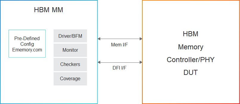
This Cadence® Verification IP (VIP) provides support for the JEDEC® High-Bandwidth Memory (HBM) DRAM device standard. It provides a mature, highly capable compliance verification solution that supports simulation, formal analysis, and hardware acceleration platforms, making it applicable to intellectual property (IP), system-on-chip (SoC), and system-level verification. The Memory Model for HBM models a single channel of HBM DRAM; this model can be replicated for multiple channels and multiple ranks. The Memory Model for HBM runs on all leading simulators, and leverages the industry-standard Cadence Memory Model core architecture, interface, and use model.
The HBM DRAM standard is an industry-leading, low-power, double-data-rate, high-data-width, volatile (DRAM) device memory standard for storage of system code, software applications, and user data. The HBM DRAM Memory Device Standard is designed to satisfy the performance and memory density demands of the leading-edge mobile devices. The Memory Model for HBM supports single-channel implementation version of the following HBM DRAM specifications, and can be used eight times to model a single 8-channel device.
Supported specification: The VIP for HBM Memory Model supports JEDEC specifications: JESD235B Rev 2.60 (HBM2E), JESD235B Rev 2.50 (HBM2) and JESD235 Rev 1.27 (HBM), JESD235C Rev 3.30
Product Highlights
Hundreds of protocol and timing checkers to easily catch design bugs
Hundreds of predefined configurations based on specific memory vendors' part numbers, datasheets, or generic JEDEC definitions available on ememory.com
Transaction and memory callbacks for all protocol, model states, and device memory events
Ability to optionally skip initializations
Ability to dynamically change configuration parameters
Packet tracker creation for easy debugging
Extensive functional coverage in SystemVerilog
Integrated with the DFI HBM solution for IP level verification
Plug-and-play connectivity to System Performance Analyzer for Sub-system or SoC performance verification
Support testbench language interfaces for SystemVerilog, UVM, OVM, and SystemC
Key Features
The following table describes key features from the specifications that are implemented in the VIP:
Feature Name
Description
Speed (MHz)
1800MHz (3.6 Gbps/pin)
Device Density
Supports a wide range of device densities from 1Gb to 24Gb
Size and Modes
Programmable size: Single channel can be replicated eight times to generate a 8-channel mode
Support for 1Gb, 2Gb, and 4Gb per channel in Legacy Mode; Up to 24Gb in Pseudo Channel Mode
Pseudo Channel Mode
Divides a channel into two individual sub-channels of 64 bit I/O each
8H and 12H stack
Pseudo Channel Mode 8H configuration - 8Gb, 12Gb, and 16Gb
Pseudo Channel Mode 12H configuration - 12Gb, 18Gb, and 24Gb
Row and Column Width
Higher density HBM2E configuration supported by additional CA8 and RA6 Row and Column pins
I/O Signals and Buses
All I/O signals including RD, RR, and RC are supported by HBM
Clocking and Reset
Differential clock inputs (CK_t/CK_c) and Active Low Reset Line (reset_n)
Command Decode
Mode Register Set
Precharge Same Bank, All Bank
Refresh Single Bank, Refresh All Bank
Reset, Activate
Read/Write, Read/Write with Auto Precharge
Power Down Entry, Self Refresh Entry, Power Down/Self Refresh Exit
Initialization
Initialization sequence with all the timing checks (also IEEE 1500 Stable Power Initialization). Initialization can be skipped
SID
The stack ID (SID) acts as a bank address bit in command execution
Error-Correcting Code
Support ECC with one bit per data byte; the HBM Model does not compute any ECC. ECC bits are not included in parity calculation when Write or Read DQ Parity Function is enabled
Data Mask and Data Bus Inversion
Data on the bus can be inverted during both read and write to save power; both Data Mask and Data Bus inversion features can be set through mode registers
C/A and Data Parity Check
Checks the C/A parity for each command before execution, write parity for each write data word (DQ, DM,DBI), read parity generation for each read data word
Targeted Row Refresh Mode
Refresh the rows adjacent to the TRn that encountered MAC limit; there could be one or two target rows in a bank associated to one victim row
IEEE 1500/DFT
HBM DFT support using IEEE 1500 interface feature:
LFSR, AWORD and DWORD MISR
LFSR compare (Sticky bit)
Hard Lane repair and Soft lane repair
Extest TX and Extest RX
Device ID and Temperature Instructions
Mode Register Dump Set
User configurable MBIST register
Loopback Test Mode
Supports DFT and training between the host and HBM device
Loopback Test Mode
HBM DFT support using loop back mode feature
Soft Lane Repair and Hard Lane Repair
Interconnect lane remapping to help recover functionality of the HBM stack
Lane remapping independent for each channel
Retain the remapped lane information even when power is removed from stack
Except CK_t, Ck_c , CKE and AERR, all other I/Os can be remapped using AWORD and DWORD Remapping
DWORD Repair Mode
Two Repair Mode for DWORD remapping:
In Mode 1, it is allowed to remap one lane per byte; no redundant pin is allocated in this mode, and DBI functionality is lost for that byte only, however other bytes continue to support DBI function as long as the Mode Register setting for DBI function is enabled
In Mode 2, it is allowed to remap one lane per double byte; one redundant pin (RD) per double byte is allocated in this mode, and DBI functionality is preserved
RD, RC, and RR
Support Redundant Row, Column values for AWORD Repair, and Redundant Data(4 bits) value supported for DWORD Repair functionality
Data Width
128-bit wide data bus
Pseudo channel mode with 64-bit data per pseudo channel
DDR for Command and Data Phase
Differential ck, rdqs, and wdqs
Differential clock and data referenced to strobes RDQS_t/RDQS_c and WDQS_t/WDQS_c
1 strobe pair per DWORD
Read and Write strobes for each pseudo channel are driven and read simultaneously
Bank Groups
Modeling the concept and the timing associated with back-to-back accesses to the same and different bank group
Refresh
All bank, per-bank and self-refresh; refresh timing check; Normal mode refresh, Self refresh, Temperature controller self refresh supported
Cattrip and Temp Pin
HBM cattrip and Temp Pins functionality support for Temperature-controlled Refresh and Catastrophic Temperature Sensor