The gold standard for JEDEC® SPI Nand memory device for your IP, SoC, and system-level design verification. 

In production since 2016 for many production designs.

The Cadence Memory Model Verification IP (VIP) for Flash SPI NAND provides verification of Flash NAND devices using the SPI protocol. It provides a mature, highly capable compliance verification solution applicable to intellectual property (IP), system-on-chip (SoC), and system-level verification. The VIP for SPI NAND is compatible with the industry-standard Universal Verification Methodology (UVM), runs on all leading simulators, and leverages the industry-standard Cadence Memory Model core architecture, interface, and use model.

Supported specification: GigaDevices, Macronix, Micron, Winbond, ESMT, XTX, ATO, and ZENTEL.
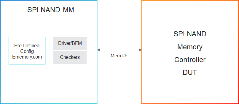
SPI NAND diagram

Product Highlights

  • Hundreds of protocol and timing checkers to catch design bugs easily
  • Hundreds of predefined configurations based on specific memory vendors' part numbers, datasheets, or generic JEDEC definitions available on ememory.com
  • Transaction and memory callbacks for all protocol, model states, and device memory events
  • Error injection capability through user modification of transaction contents
  • Ability to check for errors and change error severity
  • Ability to dynamically change configuration parameters
  • Packet tracker creation for easy debugging
  • Support testbench language interfaces for SystemVerilog and UVM

Key Features

The following table describes key features from the specifications that are implemented in the VIP:

Feature Name

Description

Operation Modes

  • Single I/O, Dual I/O, and Quad I/O (Q-SPI and QSPI) and serial mode 0 and mode 3

Pins

  • HOLD# and WP# Pins functionalities

Reset

  • Support of reset commands: 0xFF, 0xFE, which put the memory device into a known condition and to abort the command sequence in progress

Read ID

  • Support of Read ID command: 0x9F which read the identifier code (Manufacturer ID and device ID) of the memory device

Commands

  • Support of Set (0x1F) and Get (0x0F) feature: Alter device behavior for Block Protection, Lock, OTP and Configuration, and Die select register
  • Various Read commands: Page Read to Cache (0x13), Read from Cache(0x03, 0x0B Single I/O and SPI)
  • Various Program commands: Program Load (0x02), Program Execute (0x10), Program Load Random Data (0x84, 0x34, 0xC4)
  • Block Erase 0xD8 command

Page Cache Random

  • Supports of 0x30, 0xBB (Dual IO), 0xEB (Quad I/O), read page(s) in sequential/random order (Micron only)

Quad SPI

  • Quad Input and Output commands quadruple the transfer for Read and Program command, Quad SPI Mode uses DQ [3:0].
  • Read commands: Read from Cache Quad IO, Read from Cache x4
  • Program commands: Program Load x4, Program Load Random Data x4

Octal SPI/DDR

  • Octal Input and Output commands octal the transfer for Read and Program command, Octal SPI/DDR Mode uses DQ [7:0]
  • Supports Octal Double Data Rate
  • Read commands: Fast Read Octal Output, Fast Read Octal-Input/Output, DDR Fast Read Octal-Output
  • Program commands: 8-Data Input Page Data, 8-Address-Input Load Program Data, Random 8-Address-Input Load Program Data

Permanent Block Lock Protection

  • 0x2C, can lock 48 blocks per die permanently (Micron)

Simulation Test Suite

MM has a rich test suite of scenarios for easy MM evaluation and deployment.

Please contact us for further information.

Master Your Tools

Tutorials, Documentation, and Local Experts

Cadence Online Support

Increase your efficiency in using Cadence Verification IP with online trainings, VIP Portal, application notes, and troubleshooting articles