Denali Controller IP for DDR
LPDDR5/4X/4/3 and DDR5/4/3L/3, to 6400Mbps and beyond
The Cadence Denali PHY and Controller for LPDDR5X/5/4X/4/3 is a family of high-speed on-chip memory interface IP that satisfy high-performance requirements with products that are optimized for each application's needs.
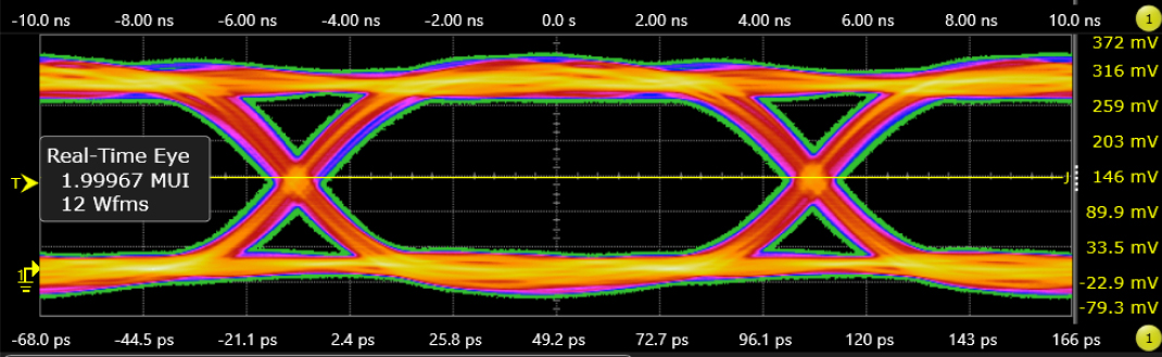
The latest LPDDR5X/5 PHY and Controller IP support the newest Low-Power Double Data Rate 5 (LPDDR5) JEDEC standard with data rates of up to 8533Mbps. The LPDDR5X/5 IP product line is a new high-speed architecture that is based on Cadence’s industry-leading LPDDR5 6400Mbps and GDDR6 22Gbps products. The architecture targets high-performance products that require low power and post-silicon programmability. The high-performance design features dynamic feedback equalization (DFE), feed foreword equalization (FFE), and continuous time linear equalization (CTLE), as well as per-bit read and write delay adjustment. Cadence’s proprietary ultra-low jitter clock trees and DLLs, proven in the GDDR6 22Gbps product line, contribute to better system timing margins, lower cost package and PCB designs, and overall system reliability. Multiple low-power modes and configurations are supported and target industry-leading exit latencies, multiple frequency set points (FSP) in hardware, and dynamic frequency scaling (DFS).
For data-intensive applications
Industry-leading PPA based on advanced architecture and implementation
Maximum system margin with advanced clocking and I/O architectures