Overview
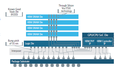
Cadence PHY IP for High-Bandwidth Memory (HBM) is leading the way with high-performance 3D-stacked DRAM system-in-package (SiP) development. Cadence’s HBM PHY IP is part of the comprehensive Cadence Design IP portfolio comprised of interface, memory, analog, and systems and peripherals IP. Cadence supports your SoC/IP integration and development with EDA tools, Palladium emulation, Verification IP (VIP), and Rapid System Bring-Up software.
Key Benefits
Proven
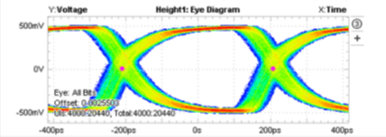
Silicon characterization reports available
Low Latency
For data-intensive applications
High Performance
8.4Gbps (HBM3E) and 3.6Gbps (HBM2E) speeds with no overdrive needed. Interposer optimized for best signal integrity.
Low Power and Area
Low power control: advanced low power modes
Full IP Integration Solutions
Rapid System Bring-Up
With other solutions, system bring-up is gated by the need for customers to write their own firmware U-Boot code in order for the SoC’s CPU to boot DRAM. This can result in the long-awaited first silicon sitting in the lab for days or weeks—after all, nothing works until the DRAM works.
However, with the Cadence Rapid System Bring-Up software, users can:
- Directly access DRAM controller and PHY registers through JTAG
- Bring up DRAM interface fast—typically in one day
- Use software that allows 2D eye shmoo on any pin—without probing
- Easily port DRAM parameters into chip-level firmware
- Allow Cadence staff to remotely and securely debug DRAM interface issues
We use Cadence LPDDR4 IP in our fast turnaround video solution for digital video consumer applications, such as cameras and TVs. We succeeded in bringing up our LPDDR4 memory subsystem with the help of Cadence DDR IP bring-up software within an hour of receiving the chip back.
– Japanese SoC vendor
We used the DDR IP bring-up software to try various IP settings and determine the optimal DDR system initialization code to be used in the firmware.
– US-based system OEM
We used Cadence bring-up software enabled on windows laptop and were able to perform training and BIST to successfully write/read/compare DDR memory. Pretty good success for just over an hour of work.
– US-based storage OEM
VIP
The Cadence Verification IP (VIP) Catalog and memory models are optimized for the IP, SoC, and system-level testing required for today's designs. All Cadence VIP come with Pureview automated configuration and TripleCheck IP Validator compliance suite for complete verification coverage of your IP within the SoC. Cadence VIP runs seamlessly on our Xcelium simulator, Palladium Z1 emulation platforms, and any third-party simulator to speed up the verification process.
The Cadence VIP portfolio supports customers developing SoCs for automotive, hyperscale data center, and mobile applications.
Emulation Models
To undertake comprehensive system-level SoC/ASIC verification, you need to stress and validate your design in a scalable verification environment—one that offers a high degree of control and visibility, applies system-level stimulus to the design, and verifies the performance and behavior of the integrated system. Using Cadence high-throughput emulation technology, design and verification teams can rapidly bring-up, verify, debug, and turn around their hardware and software designs using realistic system-level environments.
Resources