Overview
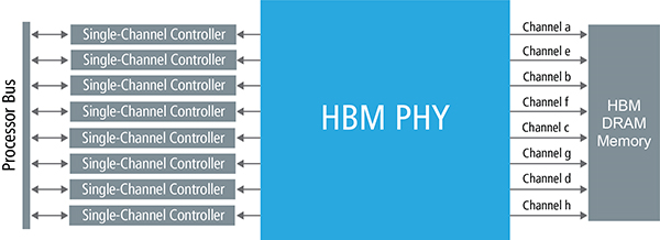
The Cadence High-Bandwidth Memory generation 2/2E PHY (HBM2E/2 PHY) is silicon-proven and is available in four process nodes: PHYs, achieving breakthrough performance, low energy per bit, and low area relative to the data bandwidth. It is engineered to quickly and easily integrate into SoCs and is verified as part of a complete memory subsystem solution. The HBM2E/2 PHY IP is an ideal solution for artificial intelligence (AI), high-performance computing (HPC), and image processing applications.

Key Benefits
Proven
Silicon characterization reports available
Low Latency
For data-intensive applications
High Performance
Highest performance HBM2E at 3.6Gbps. Interposer optimized for best signal integrity.
Low Power and Area
Low power control: advanced low power modes
Features
Resources