Overview

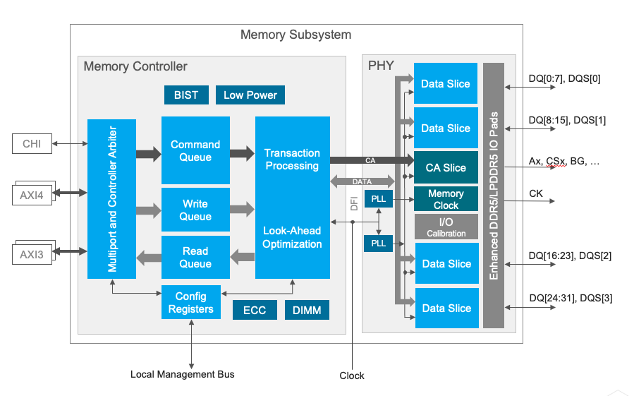
Cadence® Denali® DDR solutions, a family of high-speed on-chip interface IP, are leading the way for high-performance computing (HPC) systems and data center applications. The DDR PHY IP is engineered to quickly and easily integrate into any system-on-chip (SoC) and is verified with the Denali DDR Controller IP as part of a complete memory subsystem solution. Available as a product optimized solution for specific applications such as DDR5, DDR4, DDR3 with many configuration options to select desired features and integration aspects.

Key Benefits

Low Latency

For data-intensive applications

Low Power and Area

Industry-leading PPA based on advanced architecture and implementation

Reliable

Maximum system margin with advanced clocking and I/O architectures

Features

  • DDR5/4/3 training with write-leveling and data-eye training
  • Optional clock gating available for low-power control
  • Internal and external datapath loop-back modes
  • I/O pads with impedance calibration logic and data retention capability
  • Programmable per-bit (PVT compensated) deskew on read and write datapaths
  • RX and TX equalization for heavily loaded systems
  • Sideband and in-line SEC/DED ECC
  • Supports advanced RAS features including error scrubbing, parity, etc.
  • Compliant to LPDDR5/4X/4/3 and DDR5/4/3 protocol memories
  • Memory controller interface complies with DFI standards up to version 5.0
  • Priority per command on Arm® AMBA® 4 AXI, AMBA 3 AXI
  • Single and multi-port host interface options
  • QoS features allow command prioritization on Arm AMBA 4 AXI and CHI interfaces
  • Silicon proven and shipping in volume

Videos