Overview
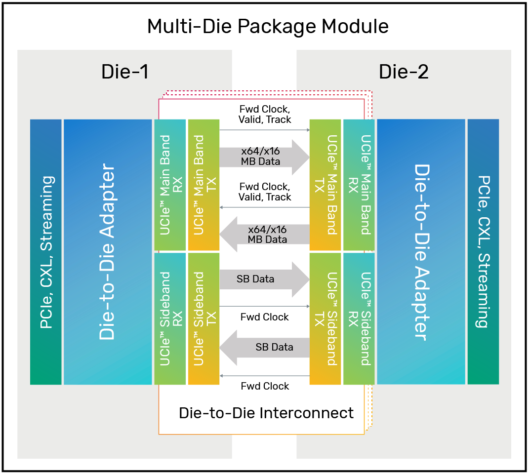
The Cadence UCIe™ PHY is a high-bandwidth, low-power and low-latency die-to-die solution that enables multi-die system in package integration for high performance compute, AI/ML, 5G, automotive and networking applications. The UCIe™ physical layer includes the link initialization, training, power management states, lane mapping, lane reversal, and scrambling. The UCIe™ controller includes the die-to-die adapter layer and the protocol layer. The adapter layer ensures reliable transfer through link state management and parameter negotiation of the protocol and flit formats. The UCIe™ architecture supports multiple standard protocols such as PCIe, CXL and streaming raw mode.

Key Benefits
Package Flexibility
Supports standard package (2D) and advanced package (2.5D)
Power Efficiency
Advanced architecture meets ultra-low power requirements
Low Latency
For data-intensive applications
High Performance Reliability
Efficient design for maximum die-to-die throughput and link data integrity
Multi-protocol Solution
Supports PCIe, CXL, and streaming protocols
Interoperability
KGD and robust test methods ensure seamless link reliability
Features
Blogs
UCIe™ is the Universal Chiplet Interconnect Express, a type of die-to-die (d2d) serial interconnect.
