Brochure
LPDDR4X/4/3/DDR4 PHY IP for TSMC 16nm/12nm
Overview
Overview
Today’s consumers generate and consume large volumes of data and video, exploding the required capacity and bandwidth for device memory. The Cadence Denali DDR family of high-speed interface IP connects to external memories with the necessary bandwidth for applications. The Cadence Denali High-Speed DDR PHY IP provides low latency and 4266Mbps throughput, while balancing power consumption and minimizing area.
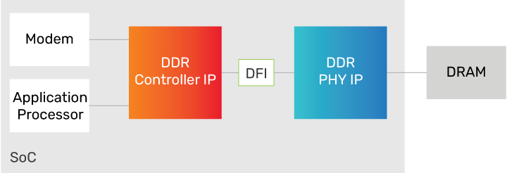
Developed by experienced teams with industry-leading domain expertise and extensively validated with multiple hardware platforms, the DDR PHY IP is silicon proven and can provide customers with ease of integration and faster time to market. The DDR PHY IP is engineered to quickly and easily integrate into any system-on-chip (SoC), and is verified with the Denali DDR Controller IP as part of a complete memory subsystem solution. The DDR PHY IP is designed to connect seamlessly and work with a thirdparty DFI-compliant memory controller.
The DDR PHY IP is developed and validated to reduce risk for the customer, so that their (SoC) can be first time right. Developed for and available early in the lifecycle of the most advanced semiconductor process nodes, the DDR PHY IP is designed to be robust under varying noise conditions and to have interoperability with various supplier memory chips.
The DDR PHY IP is part of the comprehensive Cadence Design IP portfolio comprised of interface, Denali memory interface, analog, and systems and peripherals IP.
Benefits
-
 Lowest latency for data-intensive applications
 - Highest data rates with detailed system guidelines
- Maximum system margin with advanced clocking
Product Details
The DDR PHY IP consists of a DFI interface to the memory controller, external register interface (configuration and test), PHY control block (initialization and calibration logic), and configurable data slices.
The DDR PHY IP is a high-performance DQS-delay architecture that uses programmable clock delay lines to align write data, read data capture, and DQS gating from the I/O pads across the DFI interface to the memory controller.
Key Features
- LPDDR4X/4/DDR4 training with write-leveling and data-eye training
- I/O pads with impedance calibration logic and data retention capability
- Automotive temperature grade
- Multiple PLLs for maximum system margin
- Memory controller interface complies with DFI standards 4.0 or 3.1
- Programmable clock delay (PVT compensated) on read and write datapaths for DQS alignment
- Internal and external datapath loop-back modes
- Per-bit deskew on read and write datapath
PHY Architecture
To optimize the DDR interface implementation, the DDR PHY IP provides complete flexibility with process, library, floorplan, I/O pitch, packaging, metal stack up, routing, and other physical parameters.
The DDR PHY IP is implemented with a slice-based architecture that supports a wide range of memory classes and data rates.
Data Slice and Address/Control Slices
The data slice is an 8-bit-wide design that interfaces to the DQ, DM, and DQS connections of the DRAM. The data slice is duplicated to create the appropriate data width, allowing flexibility to adjust to meet the data width requirements of the systems or applications. The address and address/control slices interface to the control, command, and address connections of the DRAM.
The address or address/control slice is duplicated to create the appropriate width for different protocols or combination of protocols, allowing flexibility to adjust the number of control, command, and address signals as needed.
External Register Interface
The external register interface is a Cadence-proprietary interface to access the data slice registers.
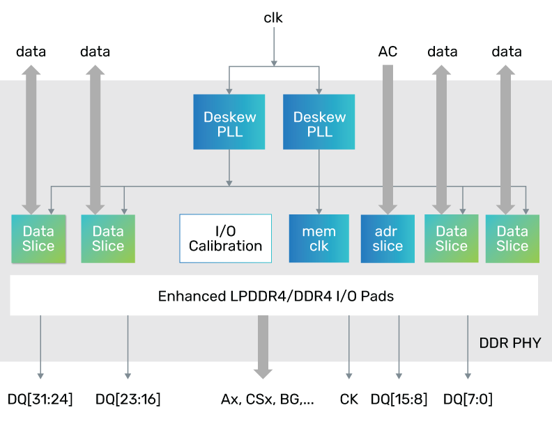
PHY Control Block
The HS PHY control block provides initialization and calibration logic for training the DQS alignment for each data slice.
Availability
The DDR PHY IP is available with various configurations and supports the following protocols:
| Protocol | Speed | Process Node |
|---|---|---|
| LPDDR4X/4/3/DDR4 | HS-4266 | TSMC 16FFC |
| LPDDR4X/4/3/DDR4 | HS-4266 | TSMC 12FFC |
Related Products
- Denali Controller IP for LPDDR4/3/2
- Denali Controller IP for DDR4/3/2
- Verification IP for Memory Models
Deliverables
- GDS II macros with abstract in LEF
- Verilog post-layout netlist
- STA scripts for use at chip or standalone PHY levels
- Liberty timing model
- SDF for back-annotated timing verification
- Verilog models of I/O pads, and RTL for all PHY modules
- Verilog testbench with memory model, configuration files, and sample tests
- Documentation, including integration and user guide, release notes
- Verification IP set-up files
For more information, visit designip