DDR/LPDDR PHY and Controller
Cadence® Denali® DDR/LPDDR PHY IP, a family of high-speed on-chip interface IP, provides the industry's highest data rates combined with low-latency throughput while balancing power consumption and minimizing area. The DDR/LPDDR PHY and Controller IP are developed and validated to reduce risk for the customer so that their SoC will work right the first time. Available as a product-optimized solution for specific applications such as DDR5/LPDDR5, DDR4/LPDDR4, DDR3/LPDDR3, and additional multiple protocol combinations.
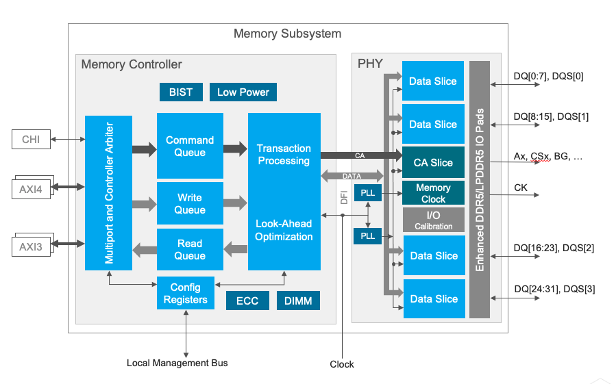
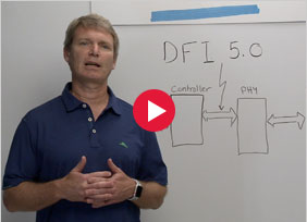
Example DDR/LPDDR PHY and Controller System
Key Benefits
Multi-protocol Solution
DDR and LPDDR supported in a single IP
Highly Configurable
Application-specific parameters and floorplan optimization
Low Power and Area
Industry-leading PPA based on advanced architecture and implementation
Low Latency
For data-intensive applications
Reliable
Maximum system margin with advanced clocking and I/O architectures
Future proof
Cutting edge technology with the latest GDDR protocols and the highest data rates