Brochure
PHY IP for HBM2 for Samsung 10LPP
Overview
Overview
Artificial intelligence (AI), high-performance computing (HPC), image processing, and autonomous driving applications generate and consume large volumes of data and require very high memory bandwidth. The Cadence Denali PHY IP for HBM2 for the Samsung 10LPP Process is an ideal solution for meeting these high-performance applications.
The PHY IP for HBM2 is comprised of architectural improvements drawn from previous-generation DDR5 and LPDDR4 PHYs, achieving breakthrough performance, low energy per bit, and low area relative to the bandwidth provided. The PHY IP for HBM2 was developed by experienced teams with industry-leading domain expertise and extensively validated with multiple hardware platforms. It is engineered to quickly and easily integrate into SoCs, and is verified with the Denali Controller IP for HBM2 as part of a complete memory subsystem solution.
Product Details
The PHY IP for HBM2 consists of a DFI interface to the memory controller for each channel, configurable PHY data slices, PHY control block (initialization and calibration logic), IEEE 1500 control block, and external register interface (configuration and test).
Benefits
-
 Derived from Cadence’s silicon-proven DDR and LPDDR IP designs
 - Achieves highest data rates with detailed system guidelines
- Delivers maximum system margin with advanced clocking and I/O architectures
Key Features
- Lowest latency for data-intensive applications
- Advanced clocking architecture minimizes clock jitter
- Highest data rates with high-resolution delay adjust
- Designed for optimized interposer routing
- Memory controller interface uses DFI 4.0-like standard
- DFI PHY Independent Mode for initialization and training
- IEEE 1500 interface, BIST module, and loop-back function
- Debug and bring-up software
PHY Architecture
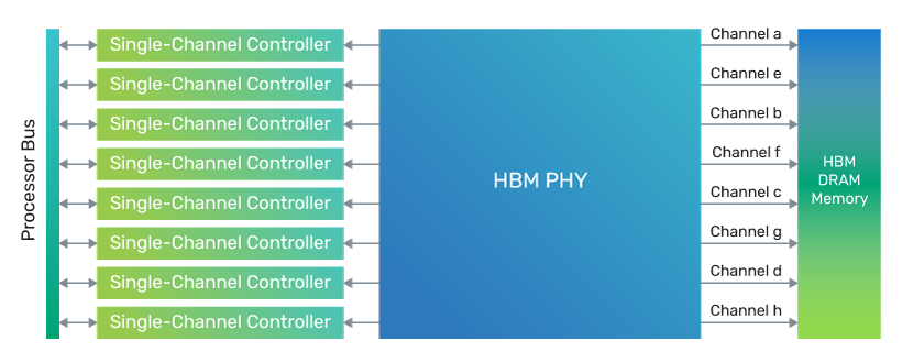
The PHY IP for HBM2 interfaces between the HBM controller and the HBM DRAM. There are eight HBM single-channel controller interfaces and eight HBM single-channel PHYs, which are all independent.
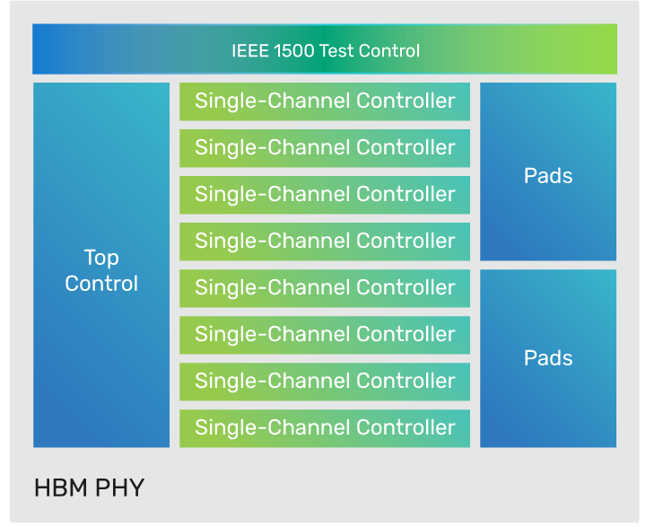
Top Control
The Top Control receives read or write requests from the controller through the external register interface. All parameters are defined through this interface to configure different features of the PHY IP for HBM2.
Single-Channel PHY
A single-channel PHY has a built-in PHY-independent (PI) leveling core, which supports training/leveling without interaction with the HBM controller.
IEEE 1500 Test Controller
The IEEE 1500 test controller provides bump connectivity testing and repair, training, temperature detection, mode register setting, and shared reset generation. It receives command requests from the PHY IP for HBM2 and implements them on the HBM DRAM stack through the standard IEEE 1500 interface. All channels of the PHY IP for HBM2 share the single test controller.
External Register Interface
The external register interface is a Cadence-proprietary interface to access the data slice registers.
Availability
The HBM2 PHY IP provides the following support:
| Protocol | Transfer Rate | Process Node |
|---|---|---|
| HBM2 | 2.4Gb/s | Samsung 10LPP |
Related Products
- Denali Controller IP for HBM2
Deliverables
- GDS II macros with abstract in LEF
- Verilog post-layout netlist
- STA scripts for use at chip or standalone PHY levels
- Liberty timing model
- SDF for back-annotated timing verification
- Verilog models of I/O pads, and RTL for all PHY modules
- Verilog testbench with memory model, configuration files, and sample tests
- Documentation—integration and user guide, release notes
- Verification IP (VIP) setup files
- Reference design for PCB and package
For more information, visit Design IP.