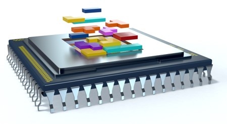
Overview
The Cadence® UltraLink™ Die-to-Die (D2D) PHY enables SoC providers to deliver more customized solutions that offer higher performance and yields while also shortening development cycles and reducing costs through greater IP reuse.
It is a mature solution that is silicon proven in multiple foundries and different process nodes.
Key Benefits
Ultra-Low Latency
Optimized for latency-sensitive applications
High Performance
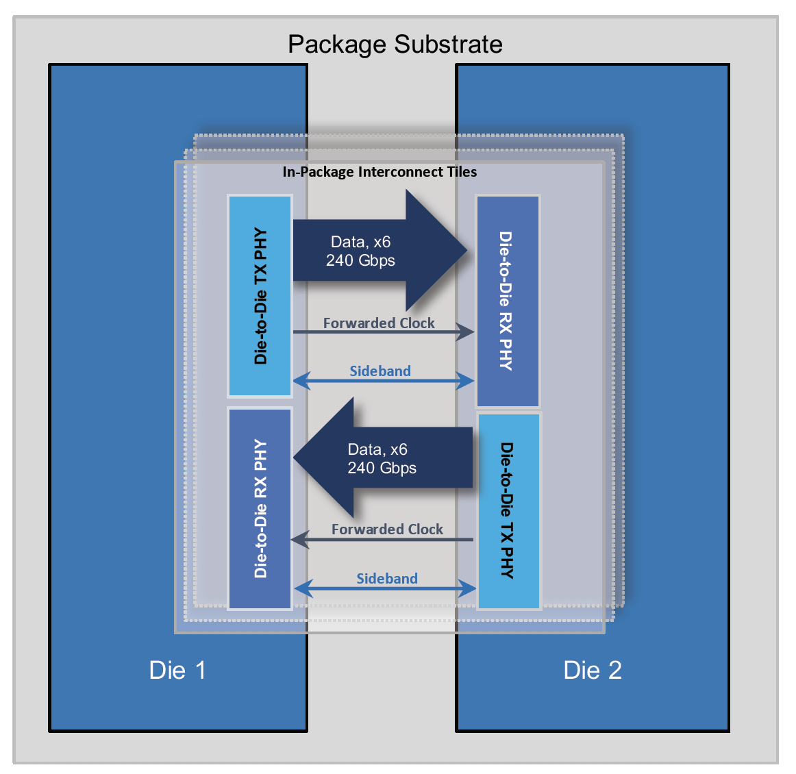
40Gbps wire speed delivers up to 1Tbps/mm unidirectional bandwidth
Cost Effective
Supports multi-chip module on organic substrates
Features