Gold standard for JEDEC® DDR4 memory device for your IP, SoC, and system-level design verification.
In production since 2011 on dozens of production designs.
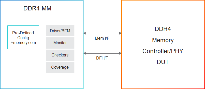
This Cadence® Verification IP (VIP) supports the JEDEC® Low Power Memory Device, DDR4 SDRAM standard. It provides a mature, highly capable compliance verification solution that supports simulation, and formal analysis, making it applicable to intellectual property (IP), system-on-chip (SoC), and system-level verification. The DDR4 SDRAM VIP is compatible with the industry-standard Universal Verification Methodology (UVM), runs on all leading simulators, and leverages the industry-standard Cadence Memory Model core architecture, interface, and use model.
DDR4 standard is the next generation of DRAM device memory standard with many improvements in performance, reliability and power saving over the previous generation of DRAM devices (DDR3). With data centers, cloud computing, and number of cores in a system increasing every day, there is a demand for high capacity and more bandwidth. With the increase in the capacity and bandwidth percentage of power consumed by memories, power consumed by the whole system is also increasing and price, performance, and watt is becoming more important as well. DDR4 addresses most of these issues with increased bandwidth, capacity, new power saving features, and with more reliability through CRC and Parity. DDR4 is not backwards compatible with DDR3.
Supported specification: JEDEC JESD79-4B specification and 3DS extensions.
Product Highlights
Hundreds of protocol and timing checkers to easily catch design bugs
Hundreds of predefined configurations based on specific memory vendors part numbers datasheets or generic JEDEC definitions available on ememory.com
Transaction and memory callbacks for all protocol, model states, and device memory events
Ability to optionally skip initializations or dynamically change configuration parameters
Packet tracker creation for easy debugging
Extensive functional coverage in SystemVerilog
Integrated with the DFI DDR5 solution for IP level verification
Plug-and-play connectivity to System Performance Analyzer for Sub-system or SoC performance verification
Support testbench language interfaces for SystemVerilog, UVM, OVM, and SystemC
Key Features
The following table describes key features from the specifications that are implemented in the VIP:
Feature Name
Description
Data Width, Density
4, 8, and 16. 2 Gb to 16 Gb
Speed
1600, 1866, 2133, 2400, 2666, and 3200
Bank Groups
Modeling the concept and the timing associated with the back-to-back accesses to the same and difference bank group
General DDR Functionality and Timing Checks
Precharge, Activate, Read, Write, Mode Register Write, Write leveling, ODT checks, Power Down, Self Refresh, Initialization, and all related timing checks
Reduced Pin Count
A16..A14 are multiplexed with ras, cas and webar pins and dedicated act pin for Activate command
Parity Error Injection
Supports Parity Error injection using callbacks
3DS Level
Supports command decoding
3DS Read and Write
Supports 3DS Read and Write commands for 2H, 4H, and 8H combinations
More Read Training Options
More MPR registers organized as pages. More options of reading those registers and preamble training
Reading of Mode Register Settings
Some important setting of the more registers are shadowed into page-2 MPRs
Data Mask and Data Bus Inversion
Data on the bus can be inverted during both read and write to save power. Both Data Mask and Data Bus inversion features can be set using mode registers
Per-DRAM Addressing
Allows mode registers of each DRAM on the DIMM to be programmed independently
CAL Mode
Allows CSBAR to be asserted a few cycles before actual command details
Write CRC
CRC is checked for writes and passes the error to the controller. CRC failures will let the write go through if Data Mask is disabled, and will block writes if that Mask is enabled
Parity
Parity checking is off by default, but when enabled parity is checked for each command before execution and also detailed recovery in case of errors and reporting of logs through MPR Reads
Control Gear Down Mode
Allows the DRAM to operate in 2N mode
Jitter, Drift, and Skews
Support of tDQSCK jitters, drift per operating voltage and temperature and skew
Configurable Preamble
Allows both 1CK and 2CK preambles to be selected for both read and write
Refresh Options
Normal mode refresh, self refresh, temperature controller self refresh, Low Power Array self refresh, and fine-granularity refresh
Maximum Power Saving Mode
Preserves the mode register settings, but loses data
RTT
Complete modelling of all RTT values, RTT_NOM, RTT_Park, and RTT_Wr with the internal register representing the value of RTT at a given point of time, based on the mode of operation
Connectivity Test Mode
Allows DRAM to enter CT Mode when Test Enable (TEN) pin is asserted HIGH