Overview
The Transition from SoCs to Chiplet-Based SoCs
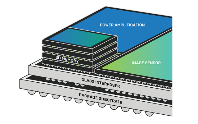
The integration of multiple heterogeneous on-package chiplets makes it easier to combine 2D and 2.5D dies from different sources, fabs, designs, and packaging technologies. This on-package mix and match of components for system-on-chip (SoC) construction is made possible by the Cadence UCIe PHY, Controller, and VIP, while leading 3D-IC tools provide designers with the full capability to improve power, performance, and area (PPA) and close timing for multi-chiplet designs using advanced or standard packages.
Key Benefits
Cadence Has the Expertise, IP, Tools, and Flows to Support You
Comprehensive Solution
The only provider that offers an integrated flow for chiplets and 3D heterogeneous integration for automotive, data center, and other verticals
Proven 3D-IC Flow
With over 25 years of advanced packaging experience, Cadence provides a comprehensive 3D-IC solution for design planning, implementation, and signoff
Features
Full-Flow IC, SiP/MCM, PCB, System Analysis, and D2D Interconnect IP
Offerings
Cadence Offers Chiplet-based SoC Design that Spans IP, Chips, Systems, and Packaging
Design IP
Cadence offers chiplet and die-to-die (D2D) connectivity solutions tailored for different applications. These solutions are designed to meet the growing demand for the disaggregated approach to chip development, which has emerged due to performance, area constraints, reticle limits, and the high cost of production at advanced nodes.
Verification
Users can enhance their verification process and boost productivity using reusable verification IP for chiplets. The Cadence Verification IP for UCIe is designed for easy integration into testbenches at the IP, chiplet, system-on-chip (SoC), and system levels.
Implementation
The Integrity 3D-IC Platform enables designers to create or import multiple chips or chiplets regardless of the technology or node they use. This platform allows system-level designers to plan, implement, and analyze any type of stacked die system for various packaging styles, such as 2.5D or 3D. This is the only integrated multi-chiplet and SoC-level solution that enables system analysis, including co-design with Cadence Virtuoso and Allegro analog and package implementation environments.
System Analysis
Since 3D-ICs are chips that are stacked on top of each other, thermal effects are magnified, making it challenging to dissipate heat in 3D stacked chiplets. Effects such as electromagnetic interference (EMI)/electromagnetic compatibility (EMC), signal integrity (SI), power, and thermal must be analyzed.
Packaging
The implementation of chiplets into system-in-packages (SiPs) presents new challenges for system architects and designers. Cadence SiP design technology enables and integrates the exploration, capture, construction, optimization, and validation of complex multi-chip and discrete substrate assemblies. This streamlines the integration of multiple high-pin count chips onto a single substrate, which is necessary for designing high-performance and complex packaging technologies.
Arm-Based Chiplets
Cadence and Arm have collaborated to create a chiplet reference design based on the UCIe standard to enable a chiplet ecosystem. This reference design provides customers the perfect starting point to create unique Arm-based chiplets in a faster and more efficient manner. These chiplets can be then plugged into the reference design for interoperability testing—a crucial step in enabling chiplets from different vendors to work seamlessly together.
The joint efforts include working together on the AMBA CHI C2C standard, the Chiplet Specification Architecture, and optimizing performance, power, and area (PPA) to speed up the design and verification processes of embedded applications such as the Scalable Open Architecture for Embedded Edge (SOAFEE).
Training and Support
Need Help?
Training
The Training Learning Maps help you get a comprehensive visual overview of learning opportunities.
Training News - Subscribe
Online Support
The Cadence Online Support (COS) system fields our entire library of accessible materials for self-study and step-by-step instruction.
Request SupportTechnical Forums
Find community on the technical forums to discuss and elaborate on your design ideas.
Find Answers in cadence technical forums

