Overview
Efficiently Design Complex Multi-Die Packages
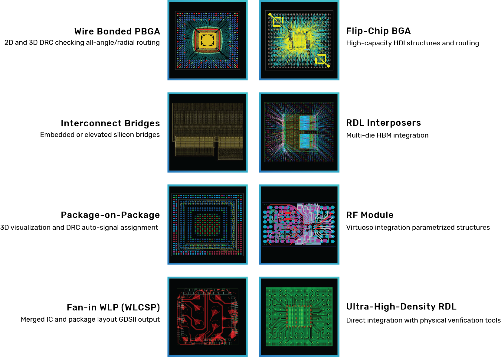
Cadence Allegro X Advanced Package Designer supports the broadest set of design rules in the industry for advanced substrates. A robust set of IC packaging-specific features are available, such as on-the-fly library development, connectivity generation/optimization, die stacking with multi-tiered wire-bonding, embedded cavities, push/shove routing, custom reports, and manufacturing outputs.


Key Benefits
Design, Characterize, Validate, and Enhance IC Packages with Unwavering Confidence
In-Design Electrical Analysis
Embedded workflows allow you to check for electrical violations such as crosstalk and IR drop without leaving the layout
First-Pass Design Success
Direct integration with Cadence Clarity 3D electromagnetic (EM) and Celsius thermal analysis engines provides streamlined path for full or partial package layouts
Seamless IC/Package Co-Design
Integrated flows with Cadence Innovus Implementation System and Virtuoso Studio enable co-design of digital and analog/RFICs and packages
Signoff Designs with Confidence
Leverage vendor assembly design kits (ADKs) for automated design setup, layout guidance, and signoff of advanced multi-die packages
Features
Empowering Intricate Designs with Seamless Multi-Die Heterogeneous Integration
Offerings
Unlock Advanced Capabilities and Go Beyond the Core Functionality
Allegro X Advanced Package Designer SiP Layout Option
A powerful extension for advanced multi-die package designs. The SiP Layout Option adds a set of auto-interactive flow, routing, and tuning features that speed planning, optimizing, routing, and timing closure of critical interconnects such as DDR, high-speed serial, silicon substrate, or graphic interfaces.
Allegro X Advanced Package Designer Silicon Layout Option
Advanced features to support ultra-high-density interconnect substrate design and verification. The Silicon Layout Option works with the Cadence Physical Verification System (PVS) to deliver flexible silicon substrate and advanced wafer-level packaging (WLP) design capabilities. It offers process development kit (PDK)-driven design rule checking (DRC), density modification and assessment, connectivity verification, and mask artwork signoff.
Allegro X PCB Symphony Team Design Option for IC Packaging
Connect multiple designers to a common SiP Layout database. The Symphony Team Design Option provides two ways for IC package design teams to collaborate—concurrent engineering using a shared canvas and distributed team design with a partitioned canvas. Either way, multiple designers can work on the same design to reduce layout time.
Training and Support
Need Help?
Training
The Training Learning Maps help you get a comprehensive visual overview of learning opportunities.
Training News - Subscribe
Online Support
The Cadence Online Support (COS) system fields our entire library of accessible materials for self-study and step-by-step instruction.
Request SupportTechnical Forums
Find community on the technical forums to discuss and elaborate on your design ideas.
Find Answers in cadence technical forums