Overview
System-Level Design Planning and Optimization - Silicon Through IC Packaging to PCB
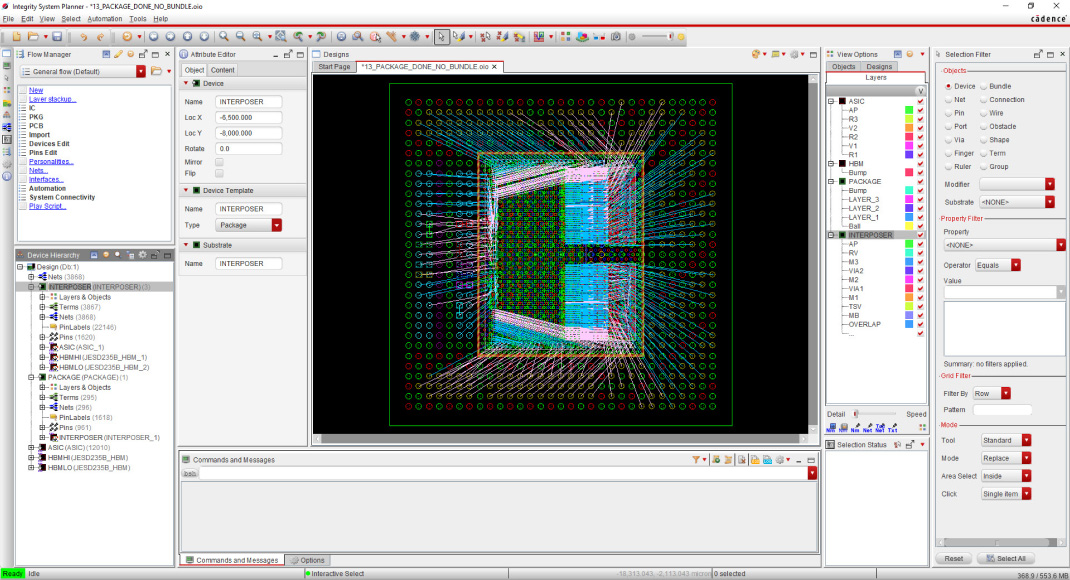
Cadence Integrity System Planner enables the entire system design process with assembly, floorplanning, connectivity definition and optimization, and physical contact layer management. Full-system connectivity visualization enables rapid exploration with the propagation of changes to adjacent substrates, providing instant feedback on the system-wide impact. Flexible connectivity definition with automatic contact pad management facilitates correct-by-design system assembly and netlist creation, eliminating separate change processes for each piece of the system.

Key Benefits
System Design Assembly, Optimization, and Management
Streamline System Design Creation and Management
Assemble and manage entire system design from one source, eliminating error-prone individual design capture and ECO processes
Instant Feedback
Full-system connectivity visualization enables rapid exploration of system-wide impact
Optimized Connection and Pin Assignment
Automatic pin assignment to assign die-to-die and die-to-substrate connections optimized for routing
Reduced Iterations
Achieve right balance of cross-substrate interconnect integration for optimal performance, cost, and manufacturability before implementation
Features
Cross-Substrate Solution for Interoperability Across Cadence Products
Training and Support
Need Help?
Training
The Training Learning Maps help you get a comprehensive visual overview of learning opportunities.
Training News - Subscribe
Online Support
The Cadence Online Support (COS) system fields our entire library of accessible materials for self-study and step-by-step instruction.
Request SupportTechnical Forums
Find community on the technical forums to discuss and elaborate on your design ideas.
Find Answers in cadence technical forums