Key Benefits
- 高效的产品创造
- 约束驱动的 PCB 设计,缩短开发周期
- 协同设计和协同分析,优化系统成本和性能
- 电气验证和签发,提高产品可靠性和管理成本
- 设计和供应链协作,有效将项目转移到制造阶段
实现高效的产品创建
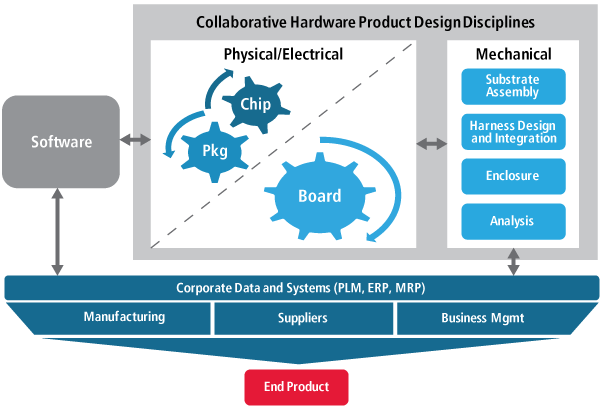
产品创建不仅仅局限于芯片或电路板设计,还应该兼顾整个产品,包括软件应用程序、机械外壳和基础电子产品。电子产品的创建过程包括团队成员之间的协作,这些协作不仅限于创作者和实现者,还包括将设计过程集成到公司系统中以及与制造合作伙伴的有效协作。
PCB 是创建成功电子产品的集成点,Cadence 提供了 Allegro® PCB 和 IC 封装设计工具以及 Sigrity™ SI/PI 分析工具,帮助您在产品创建阶段获得成功。Cadence面向产品创建的重点功能包括:
- 原理设计和约束驱动的 PCB layout、布线和调整
- 跨DIE/封装、封装/电路板和电路板/电路板的协同设计和协同分析
- MCAD-ECAD电路板-机箱协同设计
- 兼顾电源影响的电气验证和签核
- 设计和供应链协作,有效将项目转移到制造阶段
相关视频:
With the Allegro constraint-driven design flow, we are now able to take a project from design to manufacturing in four to six months, depending on the complexity of the project. This represents a more than 25% improvement in productivity from our previous process.
Michael Hu, Director of Interconnect Design Group, R&D, Huawei Technologies
The AiDT feature in Allegro PCB Designer ended our frustrations over all of the time we were spending on routing and tuning. All of hours we're saving as a team [now] can be directed toward new project requests for the business.
Sky Huang, Deputy Director of Computer-Aided Engineering, Pegatron
With Allegro TimingVision, everything is right there in front of you—this simple fact allows the routing process to be sped up dramatically, from the manual routing efforts we have seen that can take up to four weeks, down to four days.
Bill Munroe, Principal PCB Designer, Cavium