Electrothermal Simulation
What is Electrothermal Simulation?
The electrothermal simulation of electronic products is a method to accurately predict the effect of temperature (Joule heating) on the current resistance. Determining the current loss in electronic devices and systems is very important to satisfy the required performance for consumer electronics, military/aerospace applications, automotive, and hyperscalers.
Electrothermal simulation provides designers with information about the impact of Joule heating and its effect on the components within an electronic device.

The electronic components within devices fall into two categories: passive and active components. Active components can change, add, or lessen the gain of input energy, but they depend on passive components to function properly. Heat is produced from the gain in energy provided by active electronic components, which can impact component functionality. Consequently, accurately predicting the thermal behavior of electronic components is critical to ensuring their reliability and performance.
Why is Electrothermal Simulation Important?
The electrothermal simulation of electronic products is important in optimizing PCB, IC package, and system-on-chip (SoIC) designs to alleviate the stress caused by thermal issues and meet temperature requirements that will guarantee the highest quality of the end product. Thermal simulation provides information on changes in the physical properties of electronic components with changes in temperature because heat can degrade performance and reliability.
How Does Thermal Simulation Work?
In-Design Electrothermal Simulation
The electrothermal simulation of electronic products enables the thermal analysis of the package and PCBs while considering electrical factors such as current densities. Traditionally, electronic product development projects have embraced a workflow in which the detailed multiphysics electrothermal simulation, analysis, and optimization happen very late in the design process, often as the final step of verification and signoff. However, this delay inevitably leads to costly issues that derail budgets and delay time to market, as defects in requirements and performance are uncovered that require additional cycles to address these issues. Ideally, these problems should have been discovered and mitigated earlier in the design phase.
To succeed in today’s highly competitive electronics markets, electrothermal simulation, and analysis are now being integrated from the earliest stages of the design process in a methodology called “in-design analysis,” which is moving from an afterthought in the workflow to becoming an integral part of each phase of the design process at the chip, package, board, and complete system level.
In-Design Analysis for RF/Microwave
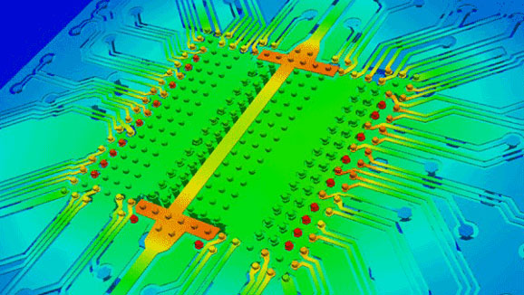
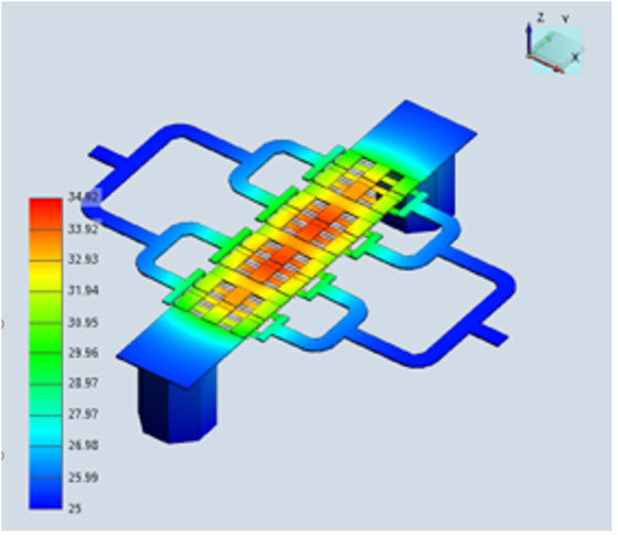
The Cadence Celsius Thermal Solver is the first electrothermal simulation technology designed for the electrical engineer. It delivers a complete electrothermal co-simulation technology for monolithic microwave ICs (MMICs), IC packages, RF PCBs, modules, and microwave/RF systems. The Celsius Thermal Solver is integrated within the Cadence AWR Design Environment platform, providing ready access to high-capacity electrothermal analysis for design verification and signoff of large, densely populated RF/microwave systems and high-power amplifiers (HPAs) (Figure 1).

The Celsius Thermal Solver’s finite-element analysis (FEA) field solver combines with advanced adaptive meshing techniques (Figure 2) to analyze steady-state heat conduction in complex solid structures, including detailed gallium nitride/gallium arsenide (GaN/GaAs) field-effect transistor (FET) and high-electron mobility-transistor (HEMT) devices with vias and airbridges, as well as complicated packages with bumps or bonding wires.
In-Design Analysis for 3D-ICs
Growing thermal and stress challenges introduced by 3D-ICs include high power density due to increased integration, non-homogenous power distribution inside the chiplet stacks, and greater thermal resistance due to the insulating dielectrics. Additionally, new stress challenges are emerging due to 3D-IC stacking, bounding, and soldering, through silicon via (TSV) drilling and filling, wafer and die thinning, and more.
3D-ICs integrate many dies (Figure 2, left) that are densely packed, which leads to heat generation, resulting in a temperature rise that causes performance issues. Consequently, it is important to accurately place the temperature sensor in the hot spot to capture and mitigate the temperature rise quickly.
The thermal challenges in packages and PCBs (Figure 2, center) are due to the Joule heating impact, IR drop, and performance. In 3D-ICs, these issues are exacerbated because of the multiple dies. In systems (Figure 2, right), it is important to have a vision of thermal performance to optimize the thermal cooling strategy. The Celsius Thermal Solver addresses these thermal heating challenges in chips, package, PCB, and system.

Electrothermal Simulation with Cadence
1. Celsius Thermal Solver – Complete electrothermal co-simulation solution
The Cadence Celsius Thermal Solver is the industry’s first complete electrical-thermal co-simulation solution for the full hierarchy of electronic systems from chips, packages, and boards to full physical enclosures. The software provides analysis and design insights that empower electrical design teams to detect and mitigate thermal issues early in the design process—reducing electronic system development iterations. Electrical-thermal co-simulation accurately simulates interrelated electrical-thermal effects. Targeting both pre-layout design and post-layout verification, the Celsius Thermal Solver enables users to quickly develop their product’s thermal management system and identify hot spots and thermal stress-related issues that are among the leading field failure risks in electronic systems.
The Celsius Thermal Solver utilizes innovative multi-physics technology to address the thermal challenges associated with complex products with greater power density. The Celsius Thermal Solver enables complete system analysis in a single tool by combining finite element analysis (FEA) for solid structures with computational fluid dynamics (CFD) for fluids.

The Celsius Thermal Solver is integrated with Cadence chip, package, and PCB design platforms, including Allegro PCB Designer, AWR Design Environment, the Innovus Implementation System, the Virtuoso System Design Platform, and the Voltus IC Power Integrity Solution. Designers can work in a single environment, share data, and enable automation between workflows and user interfaces.
