AI in Chip Design
Artificial intelligence (AI) promises to revolutionize lives. Whether it’s autonomous cars, advances in the medical industry, or simply helping identify images from your smartphone, everyone can experience this revolution. In electronics, convolution, and recurrent neural networks, and deep learning algorithms present the opportunity for an electronics revolution and a new silicon renaissance, with advances in chip design software and IP.
As technology continues to advance exponentially, semiconductor design has become increasingly complex. However, artificial intelligence (AI) is helping design engineers tackle these challenges with better results and greater efficiency than ever before. By utilizing past data, AI-driven chip design technologies offer automated insights that improve future chip designs, enhancing engineering productivity and expediting the time it takes to get products to market.
What is the significance of AI in chip design?
Key Benefits of AI in Chip Design
Ability to optimize the PPA of chips: EDA tools can help optimize power, performance, and area (PPA). This means the chip is designed to use the least amount of electricity while accomplishing its designated task. Additionally, the chip should be as small as possible to optimize space. AI technology can analyze human designs to quickly explore and identify different, optimized placements that may lead to better power consumption, performance, or use of space. By exploring different design approaches faster than humanly possible, AI algorithms can identify areas where power can be optimized and better quality of results for the design can be achieved.
Ability to automate certain chip design tasks: AI can automate chip design tasks such as place and route and debug. For example, AI can generate more optimal layouts for integrated circuits, reducing the time and effort required for this process. Optimal place and route in chip design have traditionally relied on knowledge gleaned by individual engineers over many projects. It has been a manual time-consuming process and could become even more of a bottleneck as design complexity increases. However, AI can automate the optimization of place and route task with intelligence; design engineers can ask AI algorithms to explore different place and route scenarios using different parameters and provide an optimal one for review.
Bridging the gap in chip design talent: With the global boom in electrification, the demand for semiconductor chips is growing. This requires a skilled workforce that either may not exist or may not have the years of experience required to support the complexity of designs. Here, AI tools can help bridge the workforce gap by automating aspects of the tasks that relied upon extensive prior knowledge.
How Does AI in Chip Design Work?
Reinforcement Learning (RL) is an AI technology used in chip design. RL utilizes multiple chip floor designs to achieve the best PPA configurations. The AI-generated floor plans are a product of parameters provided by electronic designers to optimize PPA through wire length reduction, congestion and density management, power consumption minimization, and area optimization. With continuous reinforcement, the RL system improves and produces better designs autonomously.
AI in Chip Design with Cadence
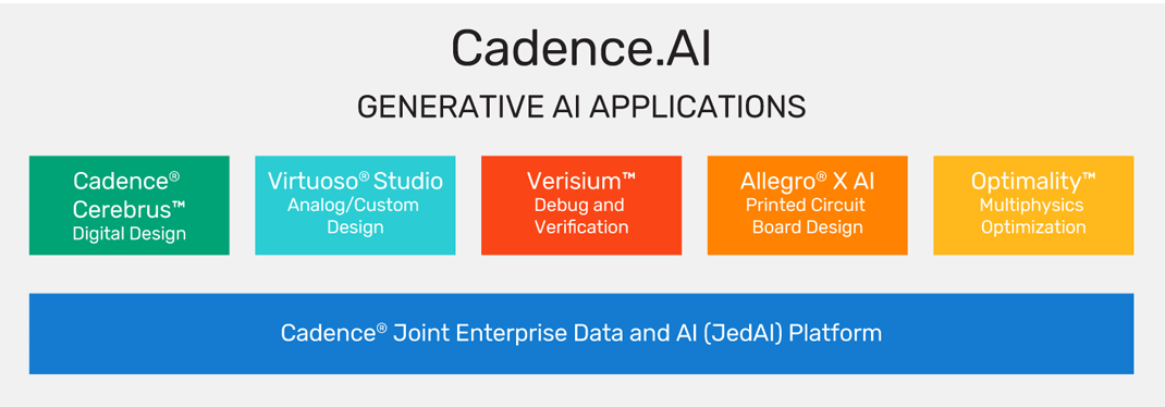
The Cadence.AI Platform is a comprehensive “chips to systems” generative AI solution that offers 10X productivity gains while optimizing system performance across all domains of design.
Cadence Allegro X AI is a revolutionary system design technology that extends the Allegro X platform with the power of artificial intelligence to enable layout automation for small to medium-sized PCBs. Allegro X AI leverages the power of cloud computing to automate four PCB tasks - placement of components, creation of power plants, routing of critical signals, and fast analysis to ensure that the produced layout is correct by construction. This level of automation enables a transformative experience. Layout tasks that took days can now be performed in hours, reducing the time to generate layout by more than 10X.
Cadence Virtuoso Studio leverages 30 years of industry knowledge and leadership in custom/analog design to provide broader support for systems, including RF, mixed-signal, photonics, and advanced heterogeneous designs. Innovative AI techniques, cloud enablement, infrastructure improvements, and integration across Cadence products complement these design flows, creating a hub for efficiently delivering designs for the real world. It supports the entire flow from chip design to advanced packaging creation to board layout. The comprehensive planar and FinFET-based automation provides better throughput and productivity—massively scalable, cloud-ready solutions for when 100s of simulations turn into 1,000s. The embedded AI-enabled tools learn and improve next-generation designs. Further, it allows the heterogeneous integration of 2.5D or 3D designs for RF and photonics systems.
The Cadence Verisium AI-Driven Platform represents a generational shift from single-run, single-engine algorithms to algorithms that leverage big data and AI across multiple runs of multiple engines throughout an entire SoC verification campaign. The Verisium platform optimizes verification workloads, boosts coverage, and accelerates root-cause analysis of bugs. The Verisium platform reduces debug turnaround time, increases debug productivity, improves regression turnaround time, and automates test-case failure triage.
Cadence Cerebrus Intelligent Chip Explorer is a revolutionary, machine learning-driven, automated approach to chip design flow optimization. Block engineers specify the design goals, and Cadence Cerebrus will intelligently optimize the Cadence digital full flow to automatically meet these power, performance, and area (PPA) goals. By adopting Cadence Cerebrus, engineers can concurrently optimize the flow for multiple blocks. This is especially important for the large, complex system-on-chip (SoC) designs needed for today’s ever more powerful electronic systems. Additionally, the engineering team's productivity improves significantly with the Cadence Cerebrus full-flow reinforcement learning technology.
Cadence Optimality Intelligent System Explorer is a multiphysics optimization software that enables the analysis and optimization realization of electronic systems. With the increasing complexity of electronic system design and greater performance requirements, Optimality Explorer surpasses the limitations of the conventional human-intensive optimization process by replacing a traditional interactive flow of design, test, and refine loop with artificial intelligence (AI)-driven technology, which expedites the optimal system design solution without compromising accuracy.
Other Cadence products that incorporate AI technology to improve their turnaround time or quality of results:


