Key Benefits
- Streamlines integration of multiple high-pin count chips onto a single substrate
- Enables early design exploration, evaluation and tradeoff analysis
- Integrates with Cadence Innovus, Virtuoso®, and Allegro® technologies
To maximize your IC package’s functional density and performance, while minimizing power consumption, Cadence® SiP Digital Architect manages the design flow from die to system-level SiP. SIP Digital Architect integrates with Cadence Innovus™ Innovation System's digital design database in a bi-directional flow for co-design optimization and makes it possible for you to author a system-level SiP connectivity mode for feasibility and verification studies.
With the market demanding more functionality than ever, SiP Digital Architect makes it possible for you to rapidly author a system-level SiP connectivity model for feasibility and verification studies. This lets you maximize the functional density and performance of the package, while minimizing power consumption. SiP Digital Architect also performs IC I/O pad-ring/array co-design with optimization capabilities at the IC, substrate, and system levels.
Features
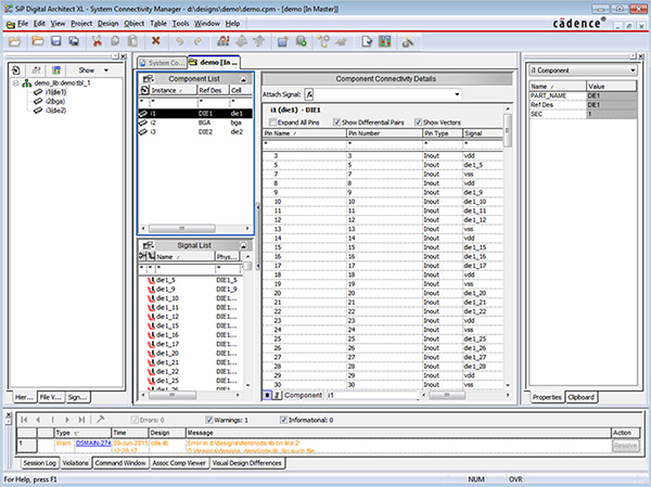
- Speeds connectivity authoring and management with unique table and spreadsheet environment
- Enables rapid system-level connectivity capture and “what-if” scenarios
- Resolves design tradeoffs early in the flow for maximum performance
- Completes I/O pad-ring/array co-design with multi-level optimization
- Supports bi-directional ECO and LVS flow for full co-design implementation
- Performs feasibility and verification studies for design optimization
- Allows RF and mixed-signal incorporation as hierarchical sub-blocks profiles
Training and Support
Need Help?
Training
The Training Learning Maps help you get a comprehensive visual overview of learning opportunities.
Training News - Subscribe
Online Support
The Cadence Online Support (COS) system fields our entire library of accessible materials for self-study and step-by-step instruction.
Request SupportTechnical Forums
Find community on the technical forums to discuss and elaborate on your design ideas.
Find Answers in cadence technical forums