Key Benefits
- 通过与 Cadence Physical Verification System 的无缝集成,提高全芯片签核效率,在单一考核中心实现完整的全芯片 DRC/LVS/ERC 审查、任务提交和错误分析
- 快速加载、编辑和分析 GDSII 和 OASIS® 的大型布局
- 易于使用的高性能独立芯片表面处理系统,支持 LEF/DEF 格式以进行数字设计审查
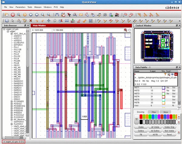
Cadence® QuickView Signoff Data Analysis Environment 是一个经过生产验证的全芯片高性能、高容量数据审查和独立芯片表面处理系统,支持多种设计格式、布局和制造数据。
QuickView Signoff Data Analysis Environment 是一个易于使用的高性能独立芯片表面处理系统,支持多种设计格式、布局和制造数据。QuickView Signoff Data Analysis Environment 可在几秒内加载大型布局(GDSII、OASIS®、LEF/DEF 和各种制造格式),提供一系列广泛的调试功能,包括网络连通性跟踪、可视化、叠层和 GDSII/OASIS® 编辑。
QuickView Signoff Data Analysis
Customers
After full-chip verification, opening the database for chip finishing can take hours, and because there are several iterations at this stage, any productivity loss has a large impact.
Tatsuji Kagatani, Department Manager, Design Automation Department System Integration, Renesas Electronics Corporation