White Paper
Thermal Warpage Simulation of a Temperature-Dependent Linear Elastic Material Package
The shift to advanced packaging in 3D and 2.5D IC design is making the numerical analysis of thermal warpage in electronic devices a crucial part of the design process. A reliable numerical tool enables the designer to perform early design analysis that accurately predicts warpage, thereby shortening the design process.
The Cadence Celsius Thermal Solver integrated within the Cadence IC, package, and PCB implementation platforms provides early-stage system analysis of thermal and stress fields. This paper demonstrates the thermal warpage simulation capability of the Celsius Thermal Solver using a semiconductor package with a temperature-dependent linear elastic material and multilayer geometry. It validates the accuracy of the solver by comparing the simulation results with flip-chip package measurements from the literature, which uses analytical solutions. The simulation results correlate well with the measurement, proving the accuracy of the Celsius Thermal Solver in performing thermal warpage analysis.
Overview
Overview
The use of simulation and analysis tools in the electronics industry is becoming increasingly mainstream due to their ability to accurately simulate next-generation technologies, such as 5G mobile networks, high-performance computing, autonomous vehicles, and the meta-universe, all of which require powerful semiconductor devices as computational units. Thermal challenges are increasing in modern electronic design, as high-temperature gradients impact power and performance and create stress and warpage in different parts of a device. It is important to understand package warpage changes over temperature to assemble reliable attached surface mount technology; otherwise, surface mount defects such as stretched joints or open joints may occur. Consequently, a reliable numerical analysis tool plays an important role in the early stage of electronic design. An accurate simulation of the design can help engineers foresee possible issues and save significant development time and costs. In line with Moore’s Law, semiconductor process technology has increased in complexity while decreasing in size. The limited space in the device makes the thermal diffusion and stress deformation of each component critical, as the deformation of the component in a tiny space will cause deflection [VPHA01], [ZPDM10]. It is precisely because of these escalating thermal challenges that the need to address them early in the design cycle that Cadence developed the Celsius Thermal Solver, the industry’s first complete electrical-thermal co-simulation tool for system analysis.
They are coupled with the key technologies that are required for stress analysis, which are, first, consideration of thermal expansion and deformation due to thermal expansion mismatch [Kon99], [SLX+08], [TCP09], [TLC19], and second, the temperature-dependent material properties. Some common components, such as underfill and epoxy, have glass transitions at specific temperature ranges, such that the mechanical properties change significantly near this range [TLHW05], [ZPDM10], [GSY+15], [SG18]. These highly temperature-dependent characteristics are usually used to reduce the deformation or warpage due to the coefficient of temperature expansion (CTE) mismatch between essential components [SLX+ 08], [HZZ10], [NA22].
The Celsius Thermal Solver provides a solution that enables multiphysics simulation at the system level with both thermal and stress analysis. This paper compares several examples with analytical solutions and shadow moire ́ experimental measurements from the literature with numerical simulation results to validate the tool’s capabilities.
Methodology
When performing stress analysis, the widely accepted physical model describes a system with stress, strain, and displacement. Stress is the force acting on a surface, while displacement represents the deformation of the solid material. The strain is a nondimensional physical parameter that evaluates the deformation of a body from a reference configuration to a current configuration. It can be broken into several parts [Bow09], representing the origin of these deformations and how they are modeled, as Equation 1 shows.
Equation 1
εtotal = εelastic + εthermal + εirreversible
εelastic is the elastic strain that describes the reversible deformation when unloading the exerting force. εthermal is the strain due to thermal expansion. εirreversible is the strain with irreversible deformation such as plasticity. This paper only considers the linear elastic model and thermal expansion are taken into consideration, such that εirreversible = 0.
Thermal strain is usually modeled with an expansion coefficient and a reference state of temperature in only volumetric contribution (no shear) of total strain (Equation 2),
Equation 2
εthermal = α(T − T0)
while α, T0 are CTE and reference temperature respectively.
For the isotropic linear elastic material, the constitutive model is described by Hooke’s law (Equation 3):
Equation 3
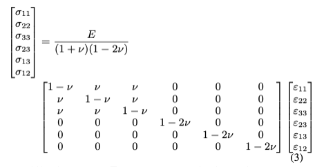
while the σ, ε , E, and ν are stress, elastic strain, Young’s modulus, and Poisson ratio, respectively.
Warpage Due to CTE Mismatch
It is common in the electronics industry to have a multilayer structure for IC packaging. A regular device usually consists of a die, substrate, PCB board, and a molding compound, and substrates are stacked by solder mask, copper, core material, and so on [HSL+17]. With different material properties, the difference in the coefficient of thermal expansion can cause strain on the package, which can generate the warpage even if the system was exerted in homogeneous temperature increments. The warpage can also cause welding failure, especially in the bridging region between the substrate and the die or between the substrate and the PCB. Figure 1 depicts a simple case to demonstrate CTE-mismatch-induced deformation, called a bimetallic strip.
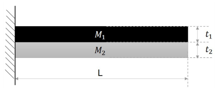
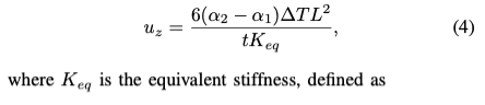
The strip consists of two different material strips with the same length and thickness. One side of the strip is fixed, and the other side is the free end. The analytical solution of the maximum deflection is provided in [YBS12], defined by the following formula in Equations 4 and 5:
Equation 4:
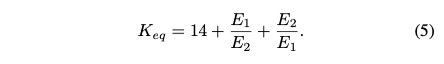
Equation 5:
Temperature-Dependent Material
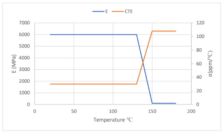
The property value is not constant for temperature-dependent material but depends on the temperature. The temperature dependency for common materials used in IC design or semiconductor manufacturing processes usually appears in Young’s modulus and CTE (e.g., E = E[T], α = α[T]) near the glass transition temperature (Tg) [Kon99], [TLHW05], [ZPDM10], [GSY+15], [HSL+17]. The temperature-dependent material property table provided in these papers usually consists of two values of Young’s modulus (or CTE) and a Tg. In [TLHW05], Figure 2 shows the simplest mathematical description of these two properties. Note that the literature does not usually provide the size of the interval of the property changing region.
To better understand the temperature-dependent structural properties, an example was simulated with an existing analytical solution to verify the solver. A rectangle bar was placed along the z-axis and boundary constraints were imposed at the top and bottom surface of the bar to confine the zero displacement in the z-direction. When the temperature of the bar increases, the bar tends to expand in the x, y direction. In this case, the stress at the surface of the x, y direction was zero (free surface), which led to a related strain in a different direction (Equation 6),
Equation 6
and the total strain in the z-direction was zero due to the boundary constraint, such that the elastic strain should be balanced with the thermal strain purely as in Equation 7:
Equation 7
In general, the stress between two temperature states can be written as Equation 8 shows:
Equation 8
In the material properties changing region in Figure 2, Young’s modulus and the CTE can be represented as a linear function of temperature (Equations 9 and 10),
Equation 9
Equation 10
while C1 is the known parameter if the material properties have been measured at T = T1 and T2. Therefore, Equation 8 for the example mentioned above can be simplified, as Equation 11 shows,
Equation 11
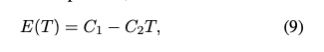
Flip-Chip Package Example
After comparing the theory and the result from the Celsius Thermal Solver, the result was validated with an industrial example, and the experimental data and the numerical result from other tools. One paper [TWL21] was selected as the primary comparison paper, as it is a clear statement on the material parameter, package geometry, and zero warpage state. Figure 3 depicts the basic die system with a square die located at the center above a square underfill and a square substrate.
The system underwent a thermal cycle as a soldering reflow process. A typical operating temperature range of the reflow process heats up from room temperature (25∼30◦C), to a higher temperature (260◦C), and then returns to room temperature. The entire system at room temperature is not flat initially due to the existence of residual stress; however, as the temperature rises, a specific temperature called the zero warpage state reduces the residual stress to zero. This state is sensitive to the case and material. According to [TWL21], the zero-warpage state is T = 120◦C observed by the shadow moire ́measurement.
Simulation Results
Deflection of the bimetallic strip
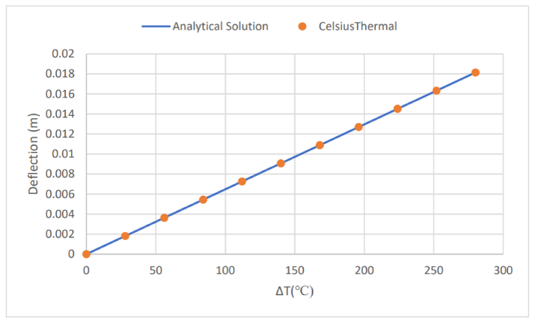
For the bimetallic strip testing example, the material properties listed in Table 1 were used and the length was set to L = 0.5m.
| Index | 1 | 2 |
|---|---|---|
| CTE (ppm/◦C) | 10.3 | 17.3 |
| Young’s Modulus (GPa) | 117.21 | 193.05 |
| Thickness (mm) | 10 | 10 |
Figure 4 shows the deflection result with respect to the temperature difference. The deflection was positive, as the CTE of material 2 is larger than that of material 1. The figure confirms a good agreement between the Celsius Thermal Solver simulation results and the theory.
Uniaxial thermal expansion with temperature-dependent properties
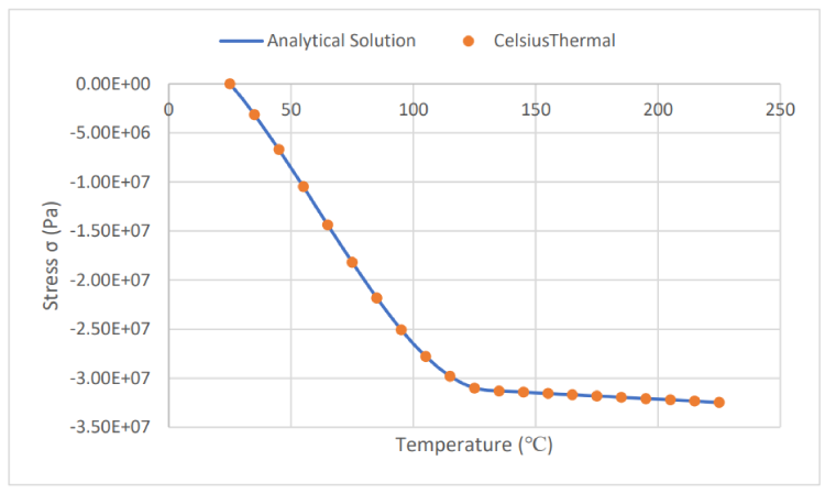
The uniaxial thermal expansion with temperature dependent properties described in the previous section with the analytical solution in Equation 11 had the material properties shown in Table 2.
| Temperature (◦C) | 25 | 130 |
| CTE (ppm/◦C) | 37.9 | 95.2 |
| Young’s Modulus (GPa) | 7.612 | 0.136 |
| Poisson’s Ratio | 0.26 | 0.26 |
These properties are assumed to be linear, depending on the temperature (Equations 9 and 10). The example was set up in the Celsius Thermal Solver, and the simulation was run with the given temperature change during the time. Figure 5 plots the stress results from the Celsius Thermal Solver compared with the analytical solution and shows that the Celsius Thermal Solver predicts the stress accurately.
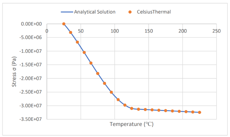
In the region T = 25 ∼ 130◦C, Young’s modulus decreases while the CTE increases, as the temperature rises. Decreasing Young’s modulus and increasing the CTE actually have a counter effect to each other on the stress estimation. The thermal strain is still increasing, but the rate of increase is less at higher temperatures. Once the temperature exceeds 130◦C, the material properties reach their new equilibrium state and remain as constants. The stress increment can still be calculated from Equation 11 by setting C2 and C4 as zeros.
Warpage Analysis of a Flip-Chip Package
Table 3 lists the material properties for the flip-chip package example.
| Material | Die | Bump/UF | Bump/UF |
|---|---|---|---|
| CTE (ppm/◦C) | 2.8 | 29/98 | 14.4 |
| Young’s Modulus (GPa) | 131 | 7.6/0.1 | 26 |
| Poisson’s Ratio | 0.28 | 0.32 | 0.39 |
| Tg (◦C) | - | 120 | - |
The temperature dependency of the properties was imposed on the underfill, following the description in [TLHW05]. Figures 6 and 7 show the numerical results of the system after undergoing a reflow process. In Figure 6, the Celsius Thermal Solver reported the maximum displacement at the bottom surface corner with respect to the temperature change.
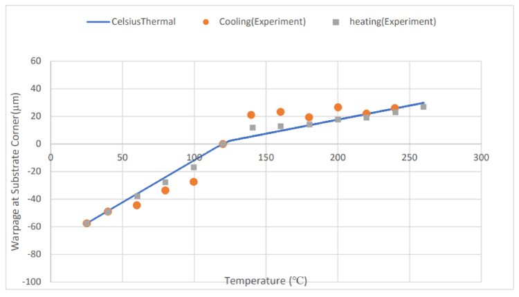
The experimental data were obtained from the literature [TWL21]. The displacement is zero at the zero-warpage state (120◦C) and this temperature marked a transition point of dramatically bending stiffness change. The warpage result from the shadow moire ́ was split into two data sets, with one being measured during the cooling process and the other during the heating process. In the numerical result, under the assumption of linear elastic material, there was not a different displacement field at the same temperature, as the thermal loading (temperature change) remained the same. Tsai’s paper [TWL21] also provides a numerical result from another tool that matched well with the result from the Celsius Thermal Solver.
In Figure 7, the spatial distribution of displacement in the z-direction along the diagonal axis from the center to the corner at the highest temperature (T = 260◦C) and the lowest temperature (T = 25◦C) were plotted and compared with the shadow moire ́measurement from the literature [TWL21]. At these two extreme temperatures, the bending direction of the package was completely opposite. The figure shows a good agreement between the numerical result of the Celsius Thermal Solver and the experimental data.
Conclusion
This paper demonstrates the capability of the Cadence Celsius Thermal Solver to accurately simulate and predict temperature-dependent material properties. The validation process uses examples with analytical solutions in two scenarios: the thermal uniaxial tension test with temperature-dependent properties and the multi-layer beam deflection due to CTE mismatch. It then presents a practical industrial case of the flip-chip package example found in the literature. Using the experimental data from this example, the maximum warpage of the system was plotted at different temperatures and spatial distribution displacements along the diagonal axis at two extreme temperatures. The result from the Celsius Thermal Solver provides a good correlation with the measurement data and matches the results from other numerical tools.
Future case studies may extend this research with further considerations, such as a setup with more complicated geometry, like a multi-layer substrate [HSL+ 17], a molded package [CMP+], and placing a package on a PCB [BXY18]. In addition, there may be more materials with temperature dependency in the system. Finally, future research can consider a nonlinear material model, such as one with viscoelastic material to replace some linear material models [LHLH11], [CSL19].
References
- [Bow09] Allan F. Bower. Applied mechanics of solids. CRC Press, 2009.
- [BXY18] Yao Bin, Wang Xiaofeng, and Zou Yabing. The study of thermally induced warpage of BGA package during reflow soldering. In 2018 19th International Conference on Electronic Packaging Technology (ICEPT), pages 1411–1414. IEEE, 2018.
- [CMP+] Fabiano A. Colling, Carlos A.M. Moraes, Celso R. Peter, Eduardo L. Rhod, Willyan Hasenkamp, Dong-Hyun Park, and Tae S. Oh. Numerical evaluation of warpage in PoP encapsulated semiconductors. In 2015 30th Symposium on Microelectronics Technology and Devices (SBMicro), pages 1–4. IEEE.
- [CSL19] Promod R. Chowdhury, Jeffrey C. Suhling, and Pradeep Lall. Characterization of viscoelastic response of underfill materials. In 2019 18th IEEE Intersociety Conference on Thermal and Thermomechanical Phenomena in Electronic Systems (ITherm), pages 1321–1331. IEEE, 2019.
- [GSY+15] Dandong Ge, N.R. Subramanian, Khai Seen Yong, Mun Yee Foo, and Swee Lee Gan. The impact of high glass transition temperature of molding compounds on power package warpage and stress performance. In 2015 IEEE 17th Electronics Pack- aging and Technology Conference (EPTC), pages 1–6. IEEE, 2015.
- [HSL+17] Jianxia Hao, Jing Shang, Xiaodong Liu, Tao Hang, Liming Gao, and Ming Li. Impact of substrate materials on packages warpage. In 2017 18th International Conference on Electronic Packaging Technology (ICEPT), pages 764–768. IEEE, 2017.
- [HZZ10] Robert L. Hubbard, Pierino Zappella, and Pukun Zhu. Flip-chip process improvements for low warpage. In 2010 Proceedings 60th Electronic Components and Technology Conference (ECTC), pages 25–30. IEEE, 2010.
- [Kon99] Mark M. Konarski. Effects of Tg and CTE on semiconductor encapsulants. Loctite Electronics, Technical paper, 1999.
- [LHLH11] Yeong-Jyh Lin, Sheng-Jye Hwang, Huei-Huang Lee, and Durn-Yuan Huang. Modeling of viscoelastic behavior of an epoxy molding compound during and after curing. IEEE Transactions on Components, Packaging and Manufacturing Technology, 1(11):1755–1760, 2011.
- [NA22] Fei Chong Ng and Mohamad Aizat Abas. Underfill flow in flip-chip encapsulation process: a review. Journal of Electronic Packaging, 144(1), 2022.
- [SG18] E. Suhir and R . Ghaffarian. Predicted thermal stress in flip-chip and fine-pitch ball-grid-array designs: Effect of the underfill glass transition temperature. J Electr Electron Syst, 7(286):2332–0796, 2018.
- [SLX+08] Peng Sun, Vincent Chi-Kuen Leung, Bin Xie, Vivian Wei Ma, and Daniel Xun-Qing Shi. Warpage reduction of package-on-package (PoP) module by material selection & process optimization. In 2008 International Conference on Electronic Packaging Technology & High-Density Packaging, pages 1–6. IEEE, 2008.
- [TCP09] Ming-Yi Tsai, Hsing-Yu Chang, and Michael Pecht. Warpage analysis of flip-chip PBGA packages subject to thermal loading. IEEE Transactions on Device and Materials Reliability, 9(3):419–424, 2009.
- [TLC19] C.H. Tsai, SW Liu, and KN Chiang. Warpage analysis of fan-out panel-level packaging using equivalent CTE. IEEE Transactions on Device and Materials Reliability, 20(1):51–57, 2019.
- [TLHW05] Ming-Yi Tsai, Yi-Chieh Lin, Chen-Yu Huang, and Jenq-Dah Wu. Thermal deformations and stresses of flip-chip BGA packages with low- and high-t/sub g/underfills. IEEE transactions on electronics packaging manufacturing, 28(4):328–337, 2005.
- [TWL21] Ming-Yi Tsai, Yu-Wen Wang, and Chia-Ming Liu. Thermally-induced deformations and warpages of flip-chip and 2.5 D IC packages measured by strain gauges. Materials, 14(13):3723, 2021.
- [VPHA01] Kaushal Verma, Seung-Bae Park, Bongtae Han, and Wade Ackerman. On the design parameters of flip-chip PBGA package assembly for optimum solder ball reliability. IEEE transactions on Components and Packaging Technologies, 24(2):300–307, 2001.
- [YBS12] Warren C. Young, Richard G. Budynas, and Ali M. Sadegh. Roark’s formulas for stress and strain. McGraw-Hill Education, 2012.
- [ZPDM10] Zhen Zhang, S.B. Park, Krishna Darbha, and Raj N. Master. Effect of glass transition slope of underfill on solder joint fatigue life. In 2010 11th International Conference on Electronic Packaging Technology & High-Density Packaging, pages 350– 355. IEEE, 2010.