White Paper
Intelligent System Design
Electronics technology is proliferating to new, creative applications and appearing in our everyday lives. To compete, system companies are increasingly designing their own semiconductor chips and semiconductor companies are delivering software stacks, enabling optimization across software and hardware for the substantial differentiation of their end products. This trend started in mobile devices and is now moving into cloud computing, automotive, and other areas. Hyperconnectivity and generation of zettabytes of data increases the importance of application-specific optimization of the silicon performance in the context of the system, as well as the system itself across the boundaries of hardware and software, analog and digital, and electrical and mechanical. In addition, many companies are including intelligence in their systems, providing services and convenience not seen until now.
Overview
Introduction
Besides designing the chip, there is a need to have the interaction with the rest of the system running and optimized. More and more systems are self-contained with communication to the outside world by some form of radio, be it 5G, Bluetooth, Wi-Fi, or another standard. Radios are among the most challenging components to design, since every design aspect depends on everything else. It is not just the shape of the antenna that is critical, but also the shape of every connector, package pin, and printed circuit board (PCB) trace. And increasingly the electronics interoperate with machines, so a holistic approach to the design and analysis of the whole system, at the system level, is required.
Design Excellence

While producing an excellent semiconductor chip has always been the goal for electronic design automation (EDA) designers, their focus has evolved over the years from just getting out a chip that worked and fit in a package, to minimizing area and cost, to minimizing power. Semiconductor processes and design tools need to be co-designed, and design excellence for a team creating a system on chip (SoC) requires optimization in many dimensions at once. Today’s electronics design involves a very complex process, a wide array of tools that transform, analyze, optimize, and verify the design throughout the process, and IP to reuse and reduce the scope of design work.
A modern system has, at its heart, one or more chips. The traditional measures of success for these chips are lowest power, highest performance, and smallest area (PPA). Area is really a surrogate for cost: the smaller the chip, the more will fit on a wafer, and the cheaper it will be to manufacture. There are other measures, too—the most critical being time to market, especially in consumer markets that are often driven by holiday shopping (a deadline that doesn’t move even if the development schedule slips). Another major constraint is the need to get the design completed with the personnel available, which almost always means fewer people than desired, who have less average experience than desired, and who are geographically distant from each other.
PPA is a concept for optimizing digital circuits. Analog, mixed-signal, and RF circuits are also sensitive to cost, performance, and area. But the quality of the representation of the signals is an additional metric measured as signal integrity (SI), and multiphysics effects such as electromagnetic, thermal, and circuit aging must also be factored in.
Reusable intellectual property (IP) components are crucial for reducing time to market for SoC projects and must be designed to achieve optimal PPA in advanced process nodes, as well as to achieve robustness for analog and multiphysics effects.
Today’s electronics design involves a very complex process, a wide array of tools that transform, analyze, optimize, and verify the design.
IP, system verification, and system validation are crucial for producing high-quality designs before the manufacturing process, assuring not only functional correctness, but also software execution performance. SoC designs can grow to be as large as multiple billions of gate logic, which stresses the verification tool capacity and throughput, as well as the very process of designing effective test stimulus and debugging.
System Innovation
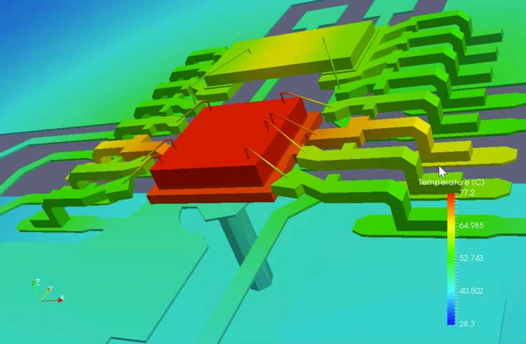
The next level up from the chips is the system itself. Some design tasks, such as PCB, chip package design, and SI analysis, have been in existence for years. But increasingly, designing each in isolation is not enough. While electronic system designers are not going to suddenly start designing phone cases or fans, modern systems require all the electronics to be analyzed in the context of the environment in which they run.
The underlying technology for system analysis is very similar to the underlying technology for things like on-chip voltage analysis, handling extremely large sparse matrices in a computationally efficient manner. In contrast to higher abstraction models, this approach is based on finite element analysis (FEA), a technique that has been around since the 1940s where physical structures are broken down into a mesh of tiny elements that are small enough to be analyzed separately and combined, and computational fluid geometry for analyzing air and water then cooling accurately.
Another system analysis technology, computational fluid dynamics (CFD), is used to characterize the flow of fluids, such as liquids and gases, inside and around physical products. Popular applications include external aerodynamics in the aerospace and automotive industries as well as propulsion and power generation by turbomachinery. These new analysis domains present the opportunity to optimize the convergence of electronic and mechanical systems.
With Moore’s Law slowing down, it has become increasingly attractive to implement big systems using chiplets, pieces of silicon functionality implemented on separate die that are integrated into a whole system on a 3D packaging substrate of some sort. There are economic benefits of using older process nodes for some portions of the design, especially if they involve analog or other specialized blocks. Often known as “More than Moore”, this can range from adding high-bandwidth memory inside the same package, up to partitioning designs into a part that needs the most advanced semiconductor technology process (perhaps the main processor) and a part that can be implemented in a less expensive older semiconductor technology process (perhaps all the communication and networking connectivity). There are various technologies that are used for the in-package communication, such as interposers for routing connections between two die, and punching signals through the chips using through-silicon vias (TSVs). These 3D systems with multiple die require a much more integrated design flow tying together some aspects of chip design (especially TSV placement), with package design, board design, and system analysis.
Another big aspect of system innovation is software. When creating new software for an existing laptop or a smartphone, the software can simply be tested on the device. When creating software for a device with an SoC that doesn’t yet exist, that approach will not work. And new software development must occur in parallel with silicon availability, a “shift left” from the traditional serial process, to ensure correct function as well as to optimize the overall schedule. The interaction of software with the underlying chips can be very complex—think of a smartphone that can make calls, take pictures, recognize your face, and play a video…all at the same time. Many rare or error conditions cannot be created with actual silicon chips—they require a “digital twin” for development of the device, a virtual representation of the actual chip under development that allows predictable and repeatable execution.
Modern systems require all the electronics to be analyzed in the context of the environment in which they run.
Security of operation is a critical issue for all electronics systems. It begins with design of secure embedded software execution, which today always starts from a secure part of the chip known as a hardware root of trust. Operating systems can also be built with security in mind, to provide reliable operation of systems even when faults occur. These concepts enable the design of a secure embedded system, secure communication to the cloud, and functionality over-the-air (OTA) secure software updates and monitoring of system operations.
Pervasive Intelligence

The main drivers of the semiconductor industry are automotive, industrial IoT, 5G communications, hyperscale computing, and machine learning (ML), a subset of artificial intelligence (AI). These rely on key enablers of hyperconnectivity and hyperscale data centers to manage all the data that is generated. ML is being added to many products and services, sometimes implemented by going “up to the cloud”, but increasingly implemented “at the edge” in the chips in the systems. This trend is driven by a number of forces. One is that people are more concerned with privacy and are increasingly unhappy about uploading everything to the cloud. Especially with smartphones and advanced driver assistance systems (ADAS), there is a lot of aggregate compute power at the edge, and additional latency going to the cloud and back wastes both time and power. Additional forces include reduced latency and compute considerations necessary to safely control robotics or high-speed automotive operation. Moving inference to the edge typically means special AI processors and often special chips tailored to the expected workload (voice recognition, traffic sign recognition, and so on). More recently, the latency and compute requirements have introduced the need for dedicated edge servers that allow both training and inferencing outside the core data center.
These trends don’t just provide opportunities for design groups and their products. They affect EDA tools and design flows of multiple tools or processes. Inside these tools, ML techniques can be used to improve the algorithms and user experience, and to achieve better PPA results. Billion-gate designs are literally beyond human comprehension and teams cannot scale to handle them. ML can raise the level of abstraction and partner with the members of the design team, reducing their effort. Under the hood, there often are multiple algorithms that can be used to attack a given issue, and which one is most appropriate depends on features of the design. For example, in formal verification, any proof technique that succeeds in proving a property is fine, while in routing, any router that completes the route is fine. Choosing between proof techniques and routers depends on the attributes of the design in a non-intuitive way, and ML approaches can be used to improve the selection.
Machine learning is being added to many products and services, sometimes implemented by going “up to the cloud”, but increasingly implemented “at the edge” in the chips and in the systems.
Design flows can be improved by ML, too. Historically, each run of a tool is starting from scratch with no access to the history of previous runs of the design, nor of similar designs. The tool is run, engineers inspect the result, they adjust some parameters, and the tool is run again. However, a lot of that iteration can be improved by retaining a lot more information from previous runs and automating some of the parameter adjustment, instead of retaining that information only in the design team’s brains. The ultimate goal is “no human in the loop”, where the design is begun and produces the result automatically.
Cloud Peak and Distributed Computing
Cloud computing is transforming semiconductor design, moving workloads to the cloud, and making massive compute available for computational software to work on design automation tasks. This vast compute resource is making it possible to replace limited personnel with unlimited computation and thereby increase design team productivity.
Why Cadence, Why Now
To power the technologies and products of the future, the world’s most creative companies require end-to-end solutions across chips, IP, packages, PCBs, and systems to meet demanding design requirements and deliver extraordinary products. Cadence has evolved to address these changes and has formulated the Intelligent System Design strategy for delivering its world-class computational software capabilities across all aspects of the design of electronic systems. It is built on three pillars:
-
 Design Excellence: An optimized EDA portfolio of tools and IP for semiconductor, package, and PCB design, with scalable distributed computing in the cloud
 - System Innovation: Expansion from EDA to enable early software development and optimize the complete system for security, responsiveness, power, electromagnetics, heat performance, multiphysics, and other aspects
- Pervasive Intelligence: The addition of ML technologies under the hood of both design tools and design flows, and IP for intelligence functionality in electronics systems and the enablement of intelligent AI/ML systems
Only Cadence has the deep expertise in computational software, along with the broadest, most integrated design solution, to bring Intelligent System Design to the products of the future.
