White Paper
Fixed-Point and Floating-Point FMCW Radar Signal Processing with Tensilica DSPs
Automotive Advanced Driver Assistance Systems (ADAS) applications are increasingly demanding radar modules with better capability and performance. These applications require sophisticated radar processing algorithms and powerful Digital Signal Processors (DSPs) to run them. Because these embedded systems have limited power and cost budgets, the DSP’s Instruction Set Architecture (ISA) needs to be efficient and easy to program. This paper describes how to optimize typical Frequency Modulated Continuous Wave (FMCW) radar range-doppler signal processing algorithm kernels using both fixed-point and floating-point computations on Cadence Tensilica DSPs.
Overview
Introduction
Radar technology is playing an increasingly important role in automotive ADAS applications. These applications require higher performance and more capabilities from the radar module to determine the distance, direction, and speed of targets in a multi-target scenario.
Because radar modules typically operate in multiple modes-for example, a “search mode” to scan for objects and a “track mode” to track specific objects of interest-adaptability and multi-function operation are essential. Using a programmable DSP as the radar signal processor offers many advantages. Implementing radar signal processing algorithm kernels as software modules enables functionality to be easily adapted by changing the code. However, the DSP executing these algorithms must have an efficient and well-tuned ISA to enable sophisticated processing algorithms to extract information from the radar signals.
This paper describes how to optimize algorithm kernels for FMCW radar range-doppler processing on the Cadence Tensilica ConnX B10 and ConnX B20 DSPs. ConnX B10 and B20 DSPs have a Single Instruction, Multiple Data (SIMD) architecture combined with an up-to-five-issue Very Long Instruction Word (VLIW) processing pipeline and a rich and extensible set of interfaces.
Because system parameters determine the computational complexity of the algorithms, this paper presents kernel performance in the context of a set of typical system parameters.
Optimizing signal processing algorithms for a DSP requires careful consideration of various factors. One factor is the data type and precision for implementing the algorithm kernels. The algorithm kernel should be precise enough to meet the functional requirements of the target application, that is, based on the Analog-to-Digital Converter (ADC) resolution, the amount of noise in the RF, analog front-end circuits, and the application’s target detection requirements.
Designs should minimize the local data memory requirement while ensuring that processing kernels operate on data from local memory for maximum processing efficiency. Finally, core computations should be performed efficiently, that is, minimizing compute cycles and memory accesses.
This paper describes the FMCW algorithm kernel analysis and optimizations, including Digital Beam-Forming (DBF), 2D RangeDoppler Fast Fourier Transforms (FFTs) with windowing, and 2D Constant False Alarm Rate (CFAR) kernels.
FMCW Processing Chain
The computational complexity of the algorithms depends on system parameters. This paper presents algorithm kernel performance in the context of the representative system as shown in Figure 1. This system, uses a linear sawtooth FMCW waveform.
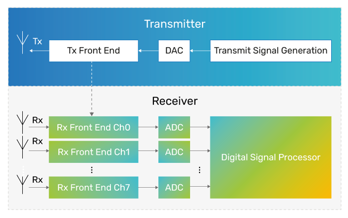
We suppose the receiver has an antenna array with 16 elements for receive Digital Beam-Forming. Each antenna array element generates one of the baseband signal’s receive channels. Figure 1 shows the transmitter as a single antenna element, but it can also be an antenna array with transmit beamforming to focus transmitted energy in beams along specific directions. The transmitted beam illuminates the desired area of interest, and we perform signal processing on the receiver end.
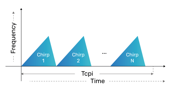
In linear sawtooth FMCW, the transmitted waveform is a sequence of linear chirp signals, and the reflected received signals are mixed with the transmitted signal to generate the beat signal. Figure 2 shows the transmitted chirp signals waveform. The beat signal is the baseband signal, sampled by the ADCs and sent to the DSP. The duration of one chirp is denoted by Tʄ and the total duration of the multiple chirp sequence transmission is called the Coherent Processing Interval (CPI), or TCPI. For one CPI, the ADCs generate a data sequence that is sampled along three dimensions: range dimension (time sampling of one chirp), doppler dimension (multiple chirps), and channel dimension (each antenna element). This three-dimensional data sequence for one CPI is the received radar data cube, which is processed by the signal processing algorithm chain on the DSP (represented in Figure 4). The sizes of the various dimensions are chosen based on the required range, speed, and direction parameters. We use the following typical system parameters:
-
 λ = 3.9mm, corresponding to 77GHz radar
 - B = 300MHz, the bandwidth sweep of one chirp
- Tʄ = 10µs
- Range maximum = 500m, Range resolution = 0.49m
- Relative speed maximum = 210km/hour
- Beat signal sampling frequency = 100Msps
- Data cube Range dimension size = 1024
- Data cube Doppler dimension size = 64
- Data cube channels dimension size (number of antenna array elements) = 16
- TCPI interval = 25ms
Implementing the Signal Processing Chain
The signal processing chain is implemented using multiple algorithm kernels optimized using the ConnX DSP ISA and stitched together to form a complete processing chain using appropriate data buffers and data flow. The data memory scheme is as follows:
- An on-chip system memory is used to store larger buffers.
- Local data memories are used for storing small, temporary working buffers.
- The optimized algorithm kernels use the local data memory buffers for input/output.
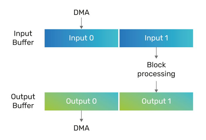
Each algorithm kernel processes data by blocks. A double buffering scheme enables data transfers between the system and local data memories in parallel to kernel processing, as shown in Figure 3.
The data block size and the tiling structure are chosen to minimize data transfers and ensure fewer transfer cycles than compute cycles, so data transfers occur fully in the background of the kernel processing.
The input data cube (range = 1024 samples, doppler = 64, and channels = 16) is generated using the system parameters listed in the FMCW Processing Chain section for scenarios with simulated targets. The output of the processing chain is verified for simulated targets.
ConnX B10 and ConnX B20 DSP Features and Configuration
The Tensilica ConnX B10 and B20 DSPs are based on an ultra-high-performance NX architecture with a 10-stage pipeline designed for use in next-generation complex signal processing applications. ConnX DSPs combine SIMD architecture with an up-to-five-issue VLIW processing pipeline and a rich and extensible set of interfaces.
The ConnX B10 DSP is built around a core vector pipeline consisting of 32 (64 for ConnX B20 DSP) 16-bit x 16-bit Multiply and Accumulate units (MACs) and a set of versatile pipelined execution units. ConnX B10 and B20 DSPs optionally support IEEE compliant single precision, half-precision, double-precision vector floating-point Fused Multiply and Adds (FMAs). Table 1 shows some of the optionally supported units in ConnX B10 and B20 DSPs.
| Tensilica ConnX DSPs | ||
|---|---|---|
| ConnX B10 | ConnX B20 | |
| 16-bit x 16-bit MACs (Double MAC) | 64 | 128 |
| 32-bit x 32-bit MACs | 16 | 32 |
| Single-precision floating point FMAs | 16 | 32 |
| Half-precision floating point FMAs | 32 | 64 |
These units support flexible precision real and complex multiply-add, bit manipulation, data shift and normalization, data select, shuffle, and interleave. ConnX B10 and B20 DSPs have a configurable instruction set with predefined, pre-verified vector packages, including FIR, FFTs, single precision vector floating point unit (SP VFP), half precision vector floating point unit (HP VFP), double precision vector floating point unit (DP VFP), and Scatter Gather. ConnX DSPs also include Xtensa 32-bit scalar ISA, ideal for efficient execution of control code. This feature makes the ConnX B10 and B20 DSPs ideal for implementing systems where high computational throughput is combined with complex decision making. For more details, please refer to ConnX B10 DSP User’s Guide and ConnX B20 DSP User’s Guide.
For simulation and cycle measurements, we use the following ConnX B10 and B20 DSP configuration:
- Two 256KB local data RAMs: internal data memories with two banks each
- 256KB local instruction RAM: internal instruction memory
- 256MB system RAM: system memory that can be accessed through a system bus
- ConnX B10 and B20 DSP ISA options enabled: Vector 32b MAC, Scatter Gather, Extended SP VFP, Extended SP VFP SP FP Add/Sub, and Extended SP VFP SP FP Reciprocal and RSQRT Accelerator
- Integrated DMA (iDMA): DMA transfers between local data RAMs and system RAM
This example of FMCW radar signal processing on the ConnX B10 and B20 DSPs is implemented as two variants:
- Variant 1 (Mixed precision): Fixed-point implementation for DBF, FFTs, and CFAR, and floating-point implementation for Angle of Arrival (AoA) using Root Multiple Signal Classification (RMUSIC) algorithm.
- Variant 2 (Float precision): Floating-point implementation for all modules.
Algorithm kernels
Figure 4 shows the signal processing algorithm chain for processing one data cube.
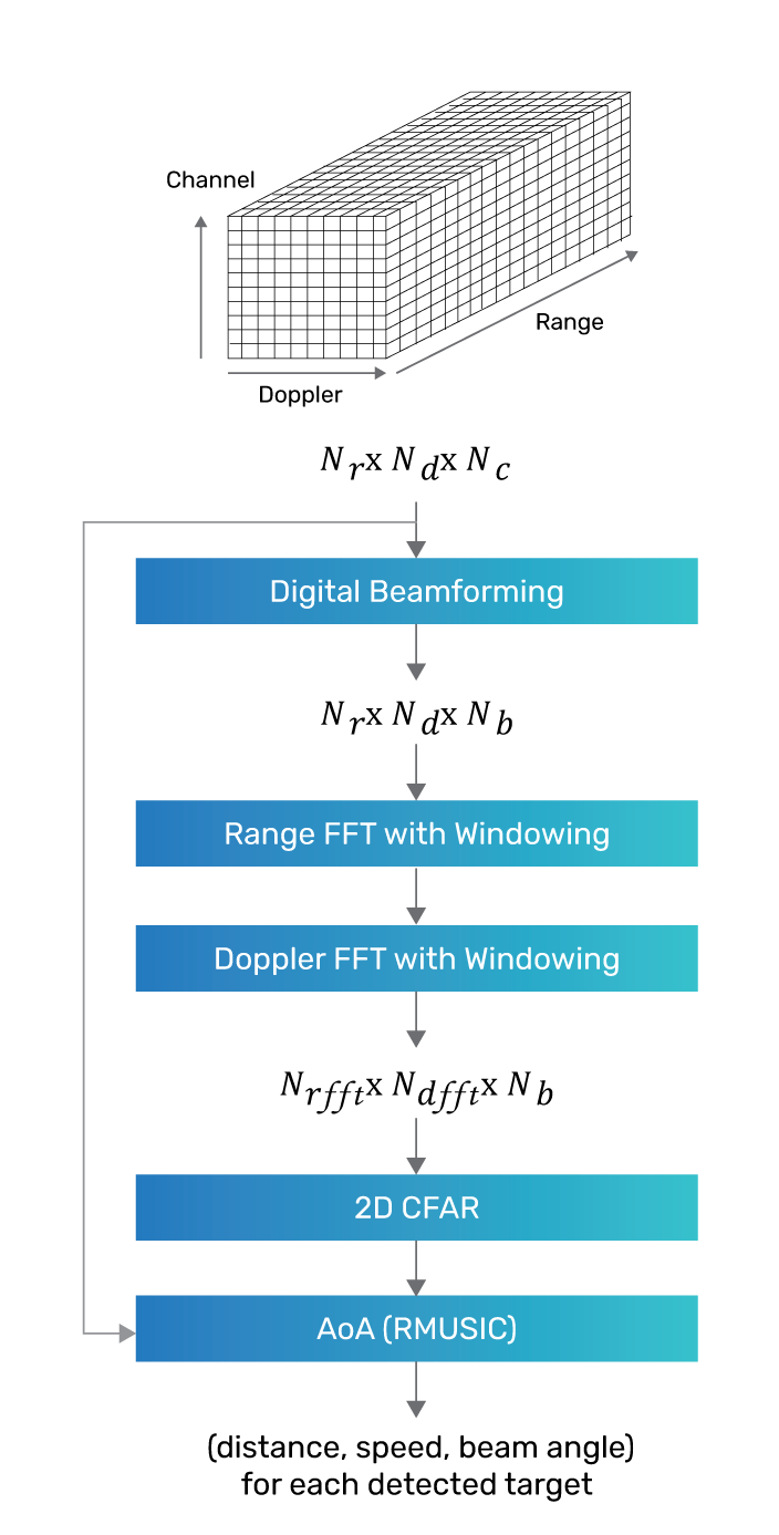
Digital Beam-forming (DBF) kernel
The DBF kernel performs FIR filtering along the channel dimension in the data cube. The length of the FIR filter is equal to the number of antenna elements (16 in this case), and the FIR taps are pre-chosen to pass signals from a beam centered on a particular pre-determined spatial direction, and suppress signals from other directions. Thus, the DBF takes the data cube as input and produces a range-doppler 2D signal as an output beam. Different sets of FIR taps can be used to generate multiple beam signals using the same data cube. We generate five beams along different directions using separate sets of FIR taps. This kernel can be implemented in Tensilica DSPs using the information in Table 2.
| Description | Fixed Point | Floating Point |
|---|---|---|
| Input data cube size | 1024x64x16 | |
| Output data cube size for five beams | 1024x64x5 | |
| Input sequence data type | Complex 16-bit fixed-point samples (represented in Q15 format) | Complex floating-point samples |
| Optimization procedure | Vectorize the core loop using the vector load, complex FIR ISA, and vector store instructions | Vectorize the core loop using the vector load, vector floating point Fused Multiply and Add (FMA), and vector store instructions |
2D Range-Doppler FFT kernel
The 2D Range-Doppler FFT kernel is used to transform each of the five 2D beam signals produced by the DBF kernel to into a 2D frequency domain spectrum. A windowed 2D FFT is used to transform the signals, with the Range FFTs along the range dimension, followed by Doppler FFTs along the doppler dimension. Each 1-D FFT uses a Hamming window.
The Range FFT is computed as a 1-D FFT, whereas the Doppler FFT is performed as a block-based FFT to avoid transposing the input and output. The FFT algorithm is based on the Decimation-in-frequency (DIF) Kronecker product-based formalization[3]. Note that the Range and Doppler FFT kernels use different block sizes. In the last stage, the Doppler FFT kernel computes the pointwise energy of each bin. The Range-Doppler FFT kernel can be implemented on Tensilica DSPs using the information in Table 3.
| Description | Fixed Point | Floating Point |
|---|---|---|
| Range-Doppler FFT kernel-Input sequence data type | Complex 16-bit fixed-point samples | Complex floating-point samples |
| Optimization procedure | Vectorize the radix-4 and radix-2 DIF butterflies using vector load-store and specialized vector FFT ISA with 16-bit fixed-point precision and dynamic scaling after each FFT stage | Vectorize the radix-4 and radix-2 DIF butterflies using vector load-store and vector FFT ISA with 32-bit floatingpoint precision |
Constant False Alarm Rate (CFAR) kernel
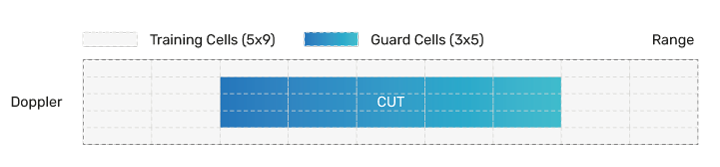
The CFAR kernel operates on the 2D energy signal in the frequency domain, classifying each bin or cell under test (CUT) in the 2D FFT energy signal either as a target bin or noise/clutter bin by comparing each CUT with a scaled estimate of noise + clutter. The scale factor and threshold used are determined by the probability of a false alarm (thus, the name CFAR). Noise + clutter is estimated by considering the cells in a rectangular neighboring region for a given CUT, leaving out some immediate neighbors of the CUT (the guard region) due to potential energy leakage from the CUT into its immediate neighbors. This implementation uses a 5x9 cell area centered at the CUT as the training region, and a 3x5 area centered at the CUT as the guard region, as Figure 5 shows.
If the CUT value is greater than the scaled noise + clutter estimate, then the CUT is classified as a target, otherwise, the CUT is classified as noise/clutter. The CFAR kernels are classified by the method used to compute noise estimate. For example, the Cell-Averaging Constant False Alarm Rate (CA-CFAR) noise estimate is formed by taking an average of the cells in the training area. In contrast, the Ordered Statistic Constant False Alarm Rate (OS-CFAR) noise estimate is formed by sorting the training area’s cell values in descending order and using the Nth sorted value. Various combinations of CA-CFAR and OS-CFAR can also be used. The AND CFAR combination does a logical AND of the classification outcomes of the CA-CFAR and OS-CFAR for each CUT, while the OR CFAR combination does a logical OR. This example uses AND CFAR. For efficient vectorization of non-linear memory accesses, we use the gather feature of ConnX B10 and B20 DSPs. The CFAR kernel can be implemented in Tensilica DSPs using the information in Table 4.
| Description | Fixed Point | Floating Point |
|---|---|---|
| Input sequence data type | 32-bit real fixed point | 32-bit real floating point |
| CA-CFAR kernel optimization procedure | Vectorize the core loop using the vector load, vector select, 32-bit fixed point vector add and vector store instructions | Vectorize the core loop using the vector load, vector select, 32-bit floating point vector add and vector store instructions |
| OS-CFAR kernel optimization procedure | Vectorize using gather instructions to load from disparate addresses, vector select, 32-bit fixed point vector min-max instructions, and vector store instructions | Vectorize using gather instructions to load from disparate addresses, vector select, 32-bit floating point vector min-max instructions, and vector store instructions |
Root Multiple Signal Classification (RMUSIC) kernel
The RMUSIC algorithm is used for frequency estimation, which calculates the precise target angle. The RMUSIC method is based on the eigenvectors of the autocorrelation matrix of the input data. It obtains the frequency estimation by examining the roots of the spectrum polynomial. The algorithm uses the Range FFT samples along the Doppler dimension (for the detected range) for all channels. To get the high-resolution AoA, typically the 32-bit single precision floating-point implementation is used. The RMUSIC kernel can be implemented in Tensilica DSPs using the information in Table 5.
| Description | Floating Point |
|---|---|
| Input sequence data type | 32-bit complex floating point |
| Optimization procedure | Vectorize the core loop using the vector load, 32-bit floating point vector complex Fused Multiply and Add (FMA), and vector store instructions |
Performance measures
Performance is computed using a test vector with a data cube dimension of 1024x64x16, five beams and six target detections, with a CPI repetition time of 25msec. Mixed precision variant 1 has a 16-bit fixed-point implementation for DBF and FFTs and a 32-bit fixed-point implementation for CFARs. The Root MUSIC algorithm requires a 32-bit floating-point implementation. This variant is best in terms of cycle performance and is a natural choice considering the precision requirements at various compute stages in the radar signal processing chain. Variant 2 has all modules implemented using a single-precision floating point. Table 6 shows the computational load in MHz for the above-mentioned test case for both variants.
| Tensilica ConnX DSPs | Computational load in MHz (for 25ms duty cycle) | |
|---|---|---|
| Variant 1 (Mixed-precision) | Variant 2 (Float-precision) | |
| ConnX B10 | 133MHz | 259MHz |
| ConnX B20 | 84MHz | 154MHz |
For more details, refer to the Implementing FMCW Radar Signal Processing Algorithms on the Tensilica ConnX B10 DSP Application Note and Implementing FMCW Radar Signal Processing Algorithms on the Tensilica ConnX B20 DSP Application Note.
Summary
This paper presents an optimized implementation of a typical FMCW radar signal processing algorithm kernels on the ConnX B10 and B20 DSPs. Performance results show that ConnX B10 and ConnX B20 DSPs with fixed-point and floating-point computations are best-suited for radar signal processing algorithms.
Additional Information
For additional information on the unique abilities and features of Cadence Tensilica processors, refer to
References
- ConnX B10 DSP User’s Guide
- ConnX B20 DSP User’s Guide
- Johnson et. al., A Methodology for Designing, Modifying, and Implementing Fourier Transform Algorithms on Various Architectures, Center for Large Scale Computation, NY 10036, Sept. 1989.
- Implementing FMCW Radar Signal Processing Algorithms on the Tensilica ConnX B10 DSP Application Note
- Implementing FMCW Radar Signal Processing Algorithms on the Tensilica ConnX B20 DSP Application Note