White Paper
Efficient Verification of Mixed-Signal SerDes IP Using UVM
Interface IP are an integral part of systems-on-chips (SoC) that include mobile, automotive, or networking applications and are primarily used for transmitting data over a physical medium between a host and device. The mixed-signal nature of the IP makes verification a challenging task, requiring special considerations for digital and analog sections. This paper describes a robust mixed-signal verification technique using the Universal Verification Methodology (UVM).
Overview
Introduction
Interface IP (SerDes) are used widely in mobile, automotive, and networking applications. These IP support low power and multiple data rates between initiator/host and responder/device communication networks to improve the link bandwidth among them. In general, the data communication may happen either within the same system or between the systems. Some SerDes designs also support features like receiver/far-end detection before establishing link communication. The latest USB Type-C is unique in that it supports a reversible cable, which means that it detects the cable orientation by determining its voltage at configuration channels. With these additional features, as well as including analog parameters, it has become critical to verify the designs against all possible operating conditions as defined by specification.
The Universal Verification Methodology (UVM) is a proven technique for functional verification. It provides the best solution to achieve metric-driven verification (MDV), which shortens the implementation and verification time by reducing redundant simulation cycles. It also provides the visibility to ensure that verification plan goals are met on scheduled time. The current digitalcentric UVM environment can verify the complex digital part of the mixedsignal IP; however, it fails to verify the analog characteristics.
In this paper, we present a robust and efficient mixed-signal verification methodology to verify SerDes designs using UVM. We also explain the modifications to standard UVM to add mixed-signal verification concepts to the methodology. With the help of new verification components that can be reused across multiple protocols with ease, mixed signal designs can be verified just as easily.
This paper also describes the implemented mixed-signal verification methodology using the USB Type-C design.
Mixed-Signal Verification Methodology
UVM is a proven verification methodology for digital-centric verification. This environment provides the following features:
-
 Reusability
 - Well-developed constrained-random stimulus
- A protocol checker
- A scoreboard for data-integrity check
- Functional coverage for stimulus quality check
This methodology can be used seamlessly for the verification of the digital content of mixed-signal designs. With minor modifications to the environment, even the analog parameters can be verified easily.
USB Type-C Standard
In this paper, we have emphasized the verification techniques needed for verifying new features specific to the USB Type-C architecture. Details of mixed-signal verification techniques used for verifying USB 3.0 PHY and USB 2.0 PHY are out of scope of this paper and are not covered.
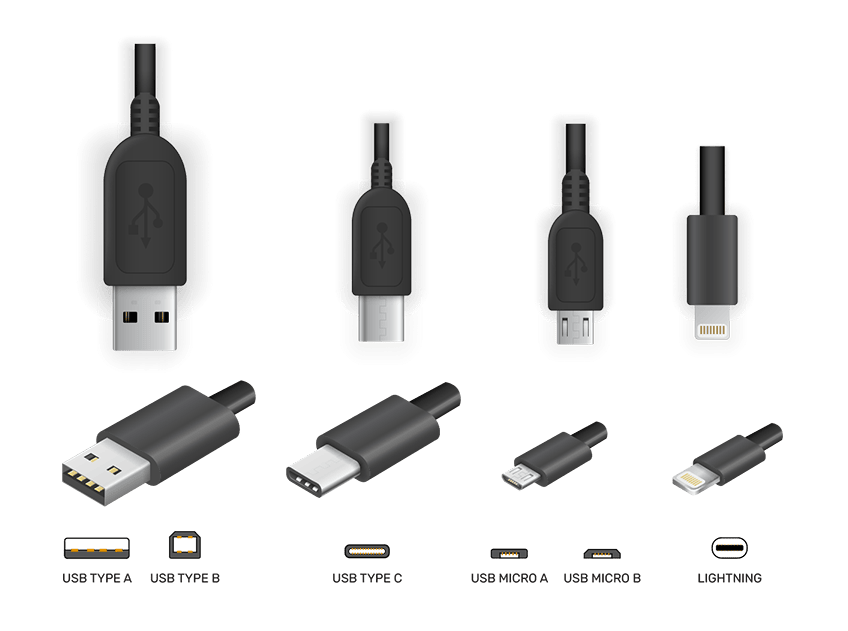
The USB Type-C standard is a smaller, thinner connector, eliminating the challenges and constraints of the large size and internal volume of the previous USB Type-A and Type-B connectors. USB Type-C also standardizes the receptacle, cable, and plug designs.
The supporting features shown in Figure 2 makes the UVM digital environment incapable of verification signoff. Designers must verify the analog characteristic behavior across all the operating modes.
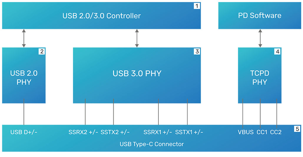
1. USB 3.0 provides the data rate of 5Gbps in SuperSpeed mode. It uses full-duplex mode of communication4.
2. USB 2.0 PHY uses half-duplex mode for communication, providing the following data rates:
- 480Mbps in high-speed (HS) mode
- 12Mbps in full-speed (FS) mode
- 1.5Mbps in low-speed (LS) modes3
3. USB Type-C PHY is predominantly in the analog domain with embedded digital domain. It needs multiple termination setups and supports the following features:
- Multiple voltage domains
- Cable orientation detection
- Multiple connection and disconnection mechanisms
4. The TCPD PHY section provides two paths to deliver power, which can be between 2.5W to 100W, depending on the USB power delivery (PD) communication2. It also performs the following tasks before the normal USB enumeration process1 :
- Plug orientation
- Cable twist detection
- DFP-to-UFP attach/detach detection
- Power relationship detection
5. The USB Type-C includes support for:
- Multiple data rates
- Power-down modes
- Half/full communication modes
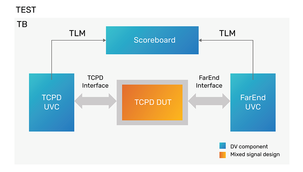
The UVM digital verification environment consists of TCPD UVC, far-end UVC, and Scoreboard. The UVM components and objects used in the environment are registered in the UVM factory. The virtual sequence controls and synchronizes the TCPD and far-end base sequences. See Figure 3.
The UVM factory method provides the ability to reuse the existing UVM digital verification environment to mixed-signal verification. This built-in factory method reduces the effort of creating a new environment for mixed-signal verification. Every registered UVM component or UVM object can be overridden by a built-in factory method (such as override by either types or instance).
Figure 4(a) shows the block diagram of a mixed-signal verification environment to verify TCPD PHY. This mixed-signal verification environment reuses the existing UVM digital verification environment. The AMS TOP UVC is the additional component developed for mixed-signal verification.
The AMS TOP UVC controls, monitors, and captures the analog characteristic behavior. This UVC is the heart of the mixed-signal verification environment and can be reused across different SerDes IP, including USB 2.0, USB 3.0, USB Type-C, and MIPI D-PHYSM with proper settings. Figure 5 shows the block diagram of the UVC.
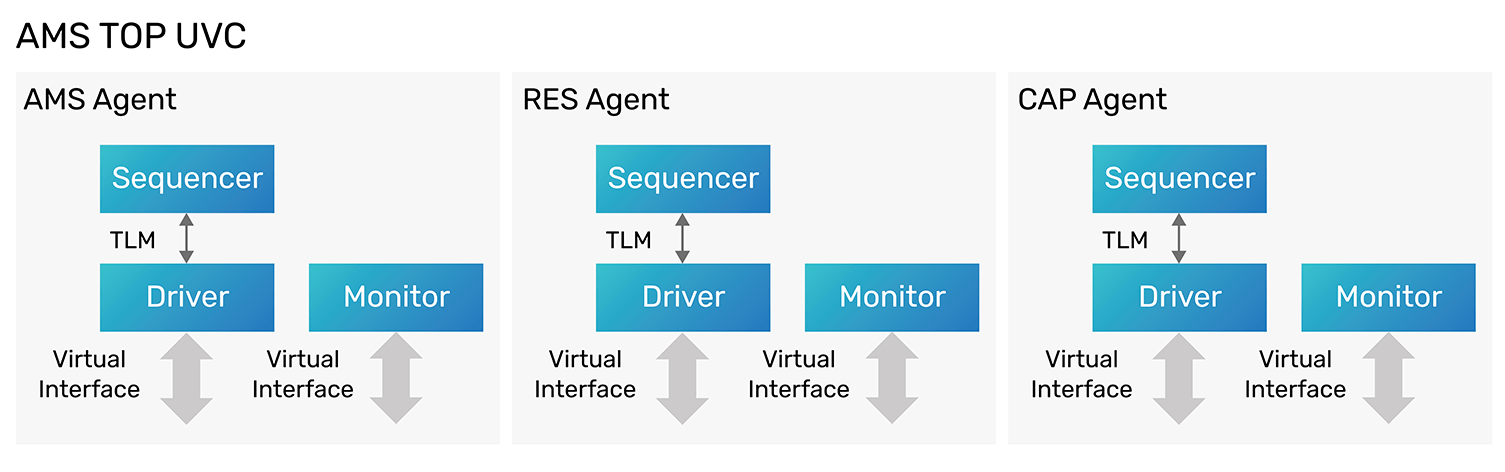
The AMS TOP UVC consists of three UVM_ACTIVE agents: the AMS agent, RES agent, and CAP agent. This block also consists of mixed-signal verification components, including:
- Pull-up circuits (CKT)
- Pull-down CKT
- Universal Connect Model (UCM)
- Analog sources
- Sample data block
The AMS TOP UVC controls the AMS agent and acts as the bridge between digital UVCs and mixed-signal components.
AMS Agent
The AMS agent controls the external environment behavior, such as supply voltage, data attenuation, and rise/fall time. This agent is embedded with a voltage-level checker and power consumption checkers. It also captures the analog characteristic variation as a functional coverage item.
RES Agent
The RES agent is used to control the resistance variation. Some of the mixed-signal SerDes IP detect the far-end device connection by monitoring the voltage on the serial lines. This voltage can vary, depending on the external device resistor. To mimic the best and worst cases, the RES agent controls the resistance variation in the environment with respect to the specification. The RES agent also captures the resistance variation as a functional coverage.
CAP Agent
The CAP agent controls the external capacitance variation in the mixed-signal environment. In USB 3.0/3.1 and PCI Express (PCIe), receiver detection is accomplished by measuring RC time constant. To mimic the best and worst cases, the CAP agent controls the capacitance variation in the environment with respect to the specification. The CAP agent also captures the capacitance variation as a functional coverage.
Pull-Up CKT
This block is used to pull-up CC1 and/or CC2 pins to represent far-end downstream-facing port (DFP). This block is controlled by the AMS and RES agents. The AMS agent controls the default current advertisement of far-end DFP. The RES agent controls the resistor values of the block.
Pull-Down CKT
This block is used to represent far-end upstream-facing port (UFP). The RES agent controls the resistor values of the block to represent different terminations.
UCM
Because the verification environment is made up of a hardware verification language (HVL), it becomes necessary to have dynamic and effective analog-to-digital (and vice-versa) conversion. This conversion is performed using a universal connect model (UCM) in the environment. The UCM is controlled by the AMS agent.
During transmission mode, analog data received on the CC1/CC2 line are converted to the logic domain and transmitted to the verification component to check the data integrity. Similarly, during the receive mode of the device under test (DUT), data being driven from the environment are converted to the analog domain before passing to the DUT. The threshold voltages, rise times, fall times, maximum amplitudes, and minimum amplitudes are parameterized and controlled by the AMS agent. The mixed-signal functional coverage bins can be added for these parameter values during regression.
An AMS verification plan (vPlan) addresses the mixed-signal parameters in the design. This verification plan helps measure the AMS verification progress along the project timeline. Figure 6(a) shows the AMS vPlan used for a USB Type-C PHY.
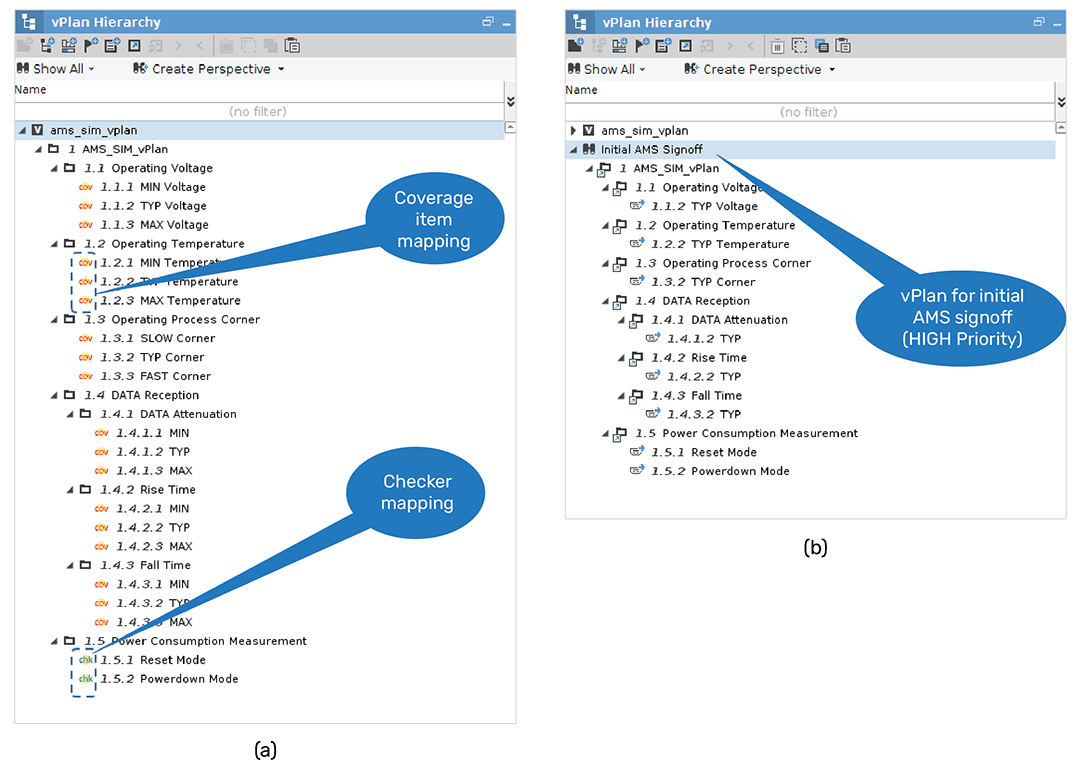
Each vPlan item is mapped to the coverage, checker, or testcase in the environment. The electrical section of the SerDes specification can be annotated to AMS vPlan items. This AMS vPlan is referred (reused) in the IP vPlan for the final verification closure and metric measurement.
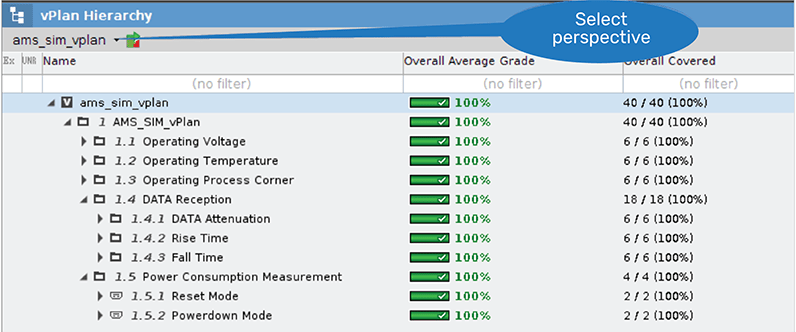
Figure 6(b) shows the perspective version of the AMS vPlan. In the verification project cycle, the AMS vPlan is used with multiple perspectives depending on the priority. This figure also shows the perspective version of AMS vPlan for initial verification signoff.
Results and Analysis
This section describes the simulation results of mixed-signal SerDes IP using a mixed-signal verification environment. For better explanation of simulation results, we compare two mixed-signal SerDes IP: USB Type-C and MIPI D-PHY.
USB Type-C PD Communication
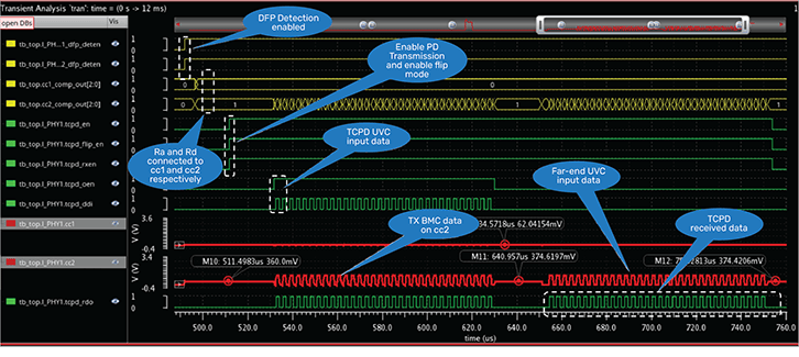
PD communication is initiated by the DFP after detecting a valid DFP-to-UFP connection and cable orientation. The DUT consists of a transmitter and a receiver that communicate across a signal CC wire depending on the cable orientation. PD communication uses half-duplex mode and a bi-phase mark coding (BMC) data transfer between the DFP and UFP. The TCPD UVC and far-end UVC both generate a randomized data packet and transmit across the CC wire. The scoreboard checks the data integrity across the CC wire. Figure 7 shows the PD communication with the “flipped” orientation.
MIPI D-PHY HS Data Transmission
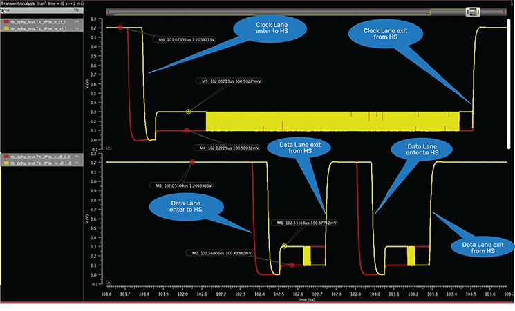
Unlike the USB/PCIe PHY, the MIPI D-PHY does not have clock data recovery block. It transmits both clock and data on separate serial lines. The clock and data lanes maintain a quadrature phase shift relationship for proper data sampling at the receiver end. The clock and data lanes drive 1.2V on a serial lane in idle mode. When the environment requests a high-speed (HS) transaction, the first clock lane enters HS mode and starts transmitting clocks on the serial lane; later, the data lane enters HS mode and begins to transmit the data payload.
Metric Measurement
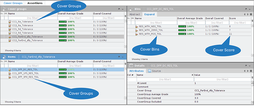
Functional coverage groups are added in a mixed-signal verification environment for the resistor ladder configuration. The RES agent captures the resistance variation on both CC1 and CC2 pins as a functional coverage. Figure 9 shows the functional coverage status for Ra, Rd, and Rp resistance variations. Figure 10 shows the AMS vPlan coverage status after the regression.
Summary and Conclusion
The UVM digital verification environment has been effectively reused for mixed-signal verification by the factory method. The scoreboard and protocol checkers are enabled in mixed-signal verification. Additional tests and functional coverage were added to the existing digital environment for robust verification of mixed-signal SerDes IP. This mixed-signal verification methodology therefore improves the verification quality and confidence in the mixedsignal design.
Acknowledgments
We would like to thank Raju Pudota, Parag Lonkar, Sumanth Chakkirala, and the Cadence Digital/AMS Verification team members for their input and valuable feedback during the implementation.
References
- USB Type-C Cable and Connector Specification (March 25, 2016), Revision 1.2
- Universal Serial Bus 2.0 Specification (April 27, 2000), Revision 2.0
- Universal Serial Bus 3.0 Specification (May 1, 2011), Revision 1.0
- Verilog-AMS Language Reference Manual (August 2008) Version 2.3, Accellera
- Varun R, Vinayak Hegde, and Somasunder Kattepura Sreenath, “Mixed-Signal Verification Methodology to Verify USB Type-C” Design and Verification Conference and Exhibition (DVCon) United States, 2017