White Paper
Building Differentiated Products Through Shorter, More Predictable Design Cycles
To position themselves for growth in today’s market, systems companies need to build highly differentiated products; reduce time to market; and focus on compliant, environmentally aware designs. This paper addresses the first two challenges—the needs to build differentiated products and reduce time to market. It discusses new design techniques, processes, and methodologies that can reduce design cycles by as much as 40%.
Overview
Introduction
With the recent global economic slowdown, system companies are facing shrinking markets and prospects with less available budget for purchasing new or the latest electronic products. Given the recent pre-downturn health of the global electronic systems market, many previously healthy high-growth and solvent companies are facing rapidly declining sales and associated revenues, deeper discounting, smaller order sizes, longer sales cycles, and increased (even hostile) competition. Many companies are making expense reductions, cancelling new or advanced projects, and reducing overhead through workforce downsizing. All of these measures are, of course, necessary in order for a business to maintain its viability. However, these alone will not drive growth in bottom-line revenue or market share. Instead, system companies are increasingly focusing on addressing a number of business challenges that, if managed successfully, can help them survive. At a macro level the three most common challenges are shown in Figure 1 below:
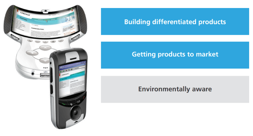
This paper will focus on the first two challenges: building differentiated products, which can enable systems companies to quickly penetrate a market, take a leadership position, and effectively counter or displace any competition; and building them faster. Clear differentiation also allows a superior value proposition, which will enable a stronger position on pricing with less need to succumb to eroding ASPs. Differentiation can involve many factors, but this paper will focus on those related to the technology impact/usage that directly enables the design of products with shorter, more predictable design cycles compared to the competition.
Needs Evolve With New Devices and Architectures
Ever since design automation tools were invented, the EDA mantra has been shorter design-cycles. First, EDA tools were compared to an Etch A Sketch, and then they were compared to themselves—previous generation tools and methodologies. So, should every release of the software just be compared to its previous version? The answer, obviously, is no. The most important comparison of a particular release of EDA vendor’s software is to compare it to the user’s / company’s design needs—i.e., How well does the new release of the PCB or IC packaging software address the design challenges the end users have?
A company’s design needs evolve as the products and services a company offers evolve. Every company wants to differentiate its offerings from its competitors, and get its products to market faster, cheaper, and with more functionality. Systems companies are also impacted by new ICs and design methodologies offered by the semiconductor industry. A good example is the introduction of serial links —such as PCI Express, Serial ATA—which change the architecture of signals on PCBs from parallel interfaces to serial interfaces. Another good example is the increasing capabilities and capacities of FPGAs, which shorten the design cycle time for system designers but add additional design challenges (pin assignment time, and increased number of iterations between PCB layout designer and FPGA designer). Pressures to reduce development costs while shortening design cycles have been forcing many companies to use low-cost geographies to do PCB designs.
Semiconductor companies often introduce new devices, interfaces, and architectures that are intended to help their systems company customers in shortening the design cycle or offering improved performance. Since their ROI lies in developing solutions that apply to the majority (not just the early few), EDA vendors and their tools tend to lag adoption of such new interfaces and architectures. When such changes are driven by standards, EDA companies can be sure that changes they make to support new interfaces—such as DDR3, DDR4, PCI Express Gen3, USB 3.1 etc.—will be applicable to a broader customer base.
When there is a need that is not supported by EDA vendors, many companies customize and/or extend EDA vendors’ tools to address their immediate needs while they wait for their EDA vendors to catch up and fill the gap. In such cases, end users need a system that is easily extensible and an EDA vendor that supports end users’ abilities to extend and customize the tool capabilities quickly and reliably.
Sharing your long-term design challenges roadmap (not your end product roadmap) makes your vendor a partner, and often allows appropriate roadmap alignment to address your needs sooner, rather than later. You should have an ongoing communication with your partner/vendor on what and how future releases being developed helps you to get what you need to shorten your design cycle
Ways to Achieve Shorter, More Predictable Design Cycles
How do PCB and IC packaging customers shorten their design cycles? There are several ways companies achieve shorter, more predictable design cycles. Although approaches vary depending on the size of the company, the market segment that the company belongs to, and its competitive position within that market segment, here are some common themes:
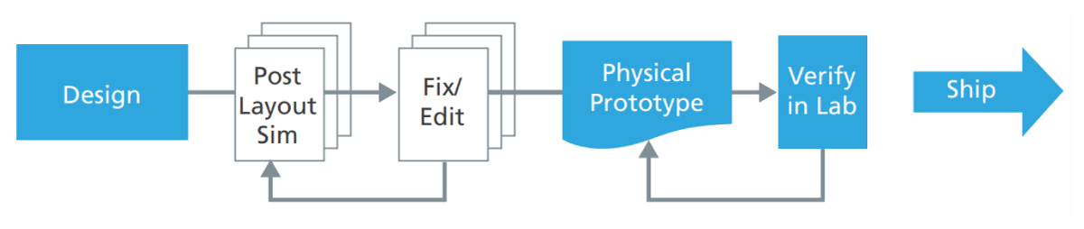
ELIMINATE UNNECESSARY DESIGN AND PHYSICAL PROTOTYPE ITERATIONS
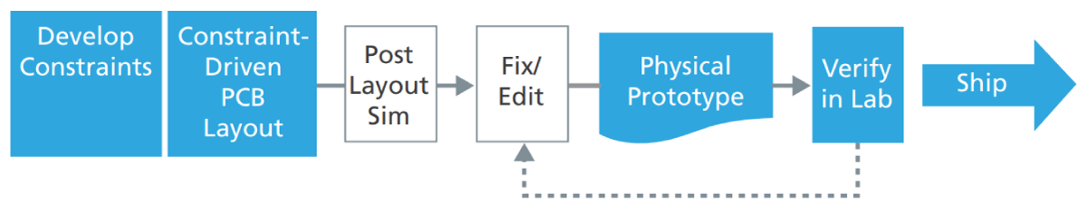
Deploy a constraint-driven design flow
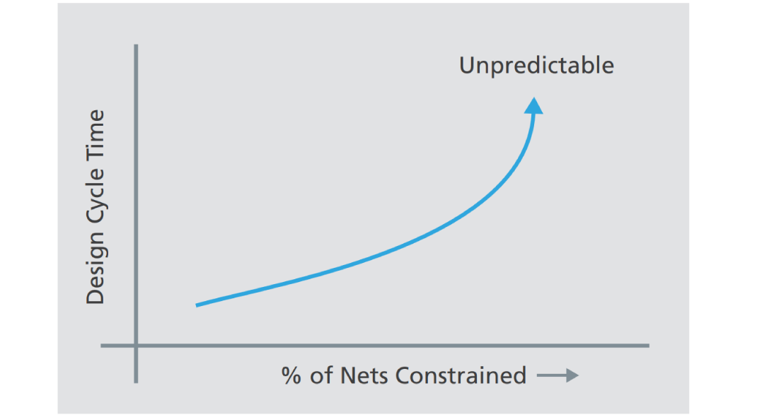
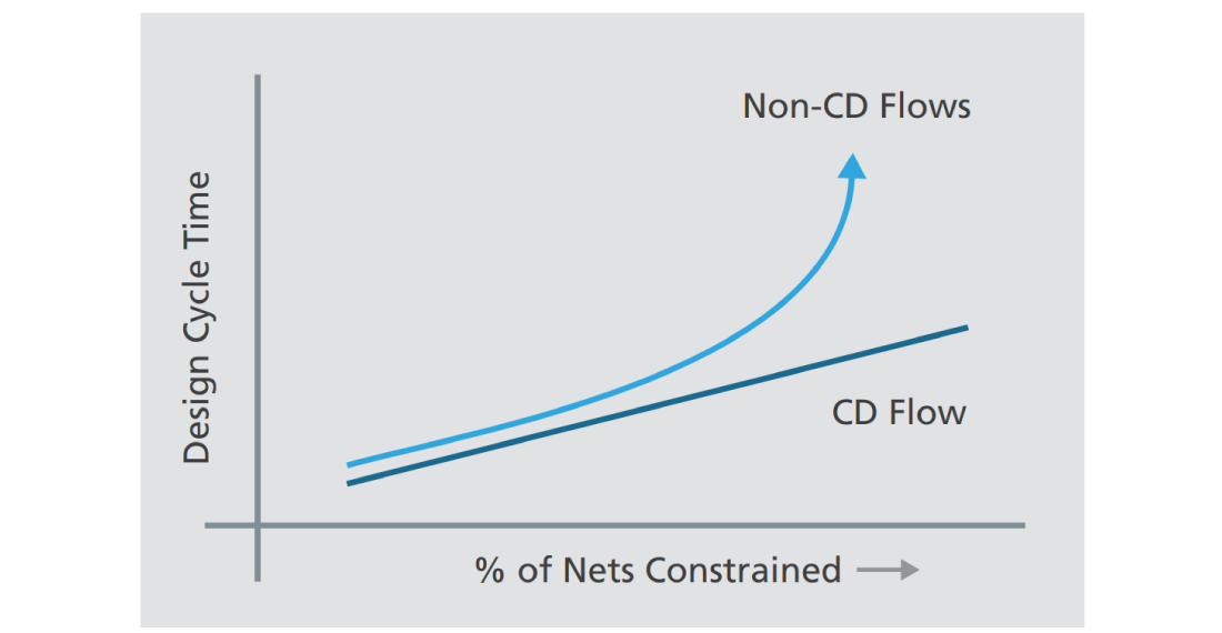
All EDA systems provide a way for incorporating traditional design manufacturing rules. Over the years, such systems have evolved to provide real-time feedback on such traditional rule adherence as the design is created and manipulated. This is the baseline. With the introduction of new devices and architectures, new design rules have to be followed. For example, using differential pairs provides some electrical advantages; they also introduce additional rules for physical implementation of such signals. Rules required to route serial links such as PCI Express Gen2 versus rules required for parallel interfaces such as DDR3 and DDR4 are very different. Often a system these days includes both serial and parallel interfaces. Having a system that allows you to specify all the rules for all such signals on your board is important. Similarly, as the manufacturing process for your designs evolves, you need a system that can combine such new rules for both manufacturing and electrical domains and guide the design as it is being developed. Having an iteration at the tail end of the design cycle—either for lack of electrical rules adherence or for lack of manufacturing rule adherence—makes the design cycle long and, worse, unpredictable.
Develop constraints through simulation to enable a constraint-driven design flow. This involves using solution space exploration to ensure development of optimal constraints for your design—these constraints, in turn, ensure that your product performs at its peak in various operating conditions. This upfront investment helps avoid iterations at the tail end of the design cycle, which could make it harder to predict when the design will be completed.
The cost of not developing such a constraint-driven design flow can either lead to several physical prototype iterations with debugging in the lab or, worse, customers finding problems with your design. The cost of physical prototype iterations varies among customers in different geographies; time lost in doing an iteration ranges from two to six weeks. Investing some of this time from one physical prototype iteration is, in and of itself, sufficient to enable a constraint-driven design flow.
Use a constraint-driven flow that supports HDI designs
Many customers are being forced to use High Density Interconnect (HDI) technology to fanout small pin pitch BGAs. BGAs with pin pitches of 0.8mm or lower usually require HDI build-up layers for fan out. A constraintdriven design flow must integrate HDI manufacturing rules with electrical rules and traditional manufacturing rules together to ensure that the design is being built correct-by-construction. Checking for fabrication rules after the design has progressed to the very end only increases the number of iterations between the tail end of the design process and doesn’t make the design cycle predictable. The solution is to use a constraint-driven flow that supports traditional manufacturing, electrical, and HDI manufacturing rules throughout the design flow.
Extend your constraint specification and management system
Use of interfaces has increased in recent years and several communities have benefited from it. Semiconductor companies reduce the risk of developing a new interface approach that may not be adopted widely. Systems companies benefit by having multiple sources for their devices that support an interface that is an industry standard. Often, the timing of introduction of a new standard like PCI Express Gen3 doesn’t coincide with the introduction of the EDA tools that support constraints required by such new standards.
The solution is to use a constraint specification system that is extensible in a manner that allows you to add your own rules. Such rules can be built on basic predicates—fundamental, atomic-level operations on objects within your designs—to allow you to customize your rules. Such rules, in most cases, can be checked as the design is modified—either interactively or automatically in batch mode.
Benefits of deploying a comprehensive constraint-driven design flow:
-
 Improved product performance and chances of first-pass success through optimum constraints. Optimum constraints are developed through explorative simulation. Upfront development of such constraints enables and drives the constraint-driven design flow.
 - Reduces time-consuming post-layout simulation to a post-layout verification step. With simulation-developed constraints that drive the constraint-driven flow, the post-layout simulation step now becomes a post-layout verification. This shortens the time required to get the design to manufacturing.
- Eliminates unnecessary physical prototype iterations. This shortens design cycle time and reduces product development costs.
- Design cycles become predictable.
ACCELERATED DESIGN AUTHORING
Design authoring has traditionally been associated with creating schematics in the EDA world. Additionally, in many instances the schematics created for simulation tend to be different than the ones used for driving the PCB layout process. Innovation in design authoring in recent years allows system designers to avoid having to author designs the same way engineers created them in the 1980s.
Design architectures have evolved since the 1980s from a common clock architecture to one that uses source synchronous interfaces (DDR3/4) and serial links (PCI Express, SATA). At the same time, with larger scale integration possible with each new advanced IC node, many FPGAs and ASSPs have far more pins than ever imagined—devices with greater than 1000 pins are becoming commonplace. Adding these large-pin-count devices on a PCB requires them to be added as a symbol in the schematics. Schematics often use company-defined sheet sizes. Fitting a 750-pin or even a 500-pin symbol is impossible in the standard sheet. Engineers and librarians are forced to represent such large-pin-count devices as multiple split symbols with labels to specify connectivity. Such split symbols are totally useless on the schematics.
Innovation in the design authoring space now allows engineers to author designs using multiple styles—tablebased for large-pin-count devices, schematics for traditional circuits with small-pin-count devices. Such approaches can shorten the design authoring time significantly—in case of backplane designs, anywhere from 10X – 20X faster than traditional schematic creation. Time to create designs with large-pin-count devices (FPGAs or ASSPs or ASICs) mixed in with traditional circuits can be accelerated anywhere between 2X – 5X, depending on the number and size of large-pin-count devices. Use the right design authoring tool to shorten your design cycle.
For mixed-signal designs or for purely analog/RF designs, often engineers use two different schematic tools: one for simulation and another for production PCB flow. This implies someone is recreating the schematics for production PCB flow. Improvements in integration between design authoring tools and simulation tools— single schematic-driven design authoring and simulation—allow engineers to avoid wasting time to recreate schematics. For RF circuits on a mixed-signal design, engineers can use a layout-driven design approach to create schematics based on the changes made to the etch elements in the layout. This eliminates the need to edit schematics manually to synchronize it with layout.
DESIGN FOR REUSE
A commonly used approach to shorten the design cycle is to reuse subsets of previous designs in new designs. Often, the next revision of a product is some modification that either reduces cost or adds some features that couldn’t be added with an earlier version—this is evolution of a product, not reuse of a subset of the design. For products that don’t fall into the evolution category, authoring the design in a manner that partitions functionality in a reusable manner can shorten the design cycle for other products. In such cases, the motivation to invest the time to partition and author designs for reuse has to come from upper management since the product team is usually focused on getting “their” product out the door quickly.
When a product has several design engineers working in parallel, such partitioning becomes a necessity and can be leveraged to create reusable blocks. Reuse can also be applied to the physical layout of the partitioned subset of the design. In such cases, it’s important to have a relationship between partitioned logic and its physical implementation. While the physical layout is tied to a specific layer stack-up, reusing the placement and etch should be easy. This reuse is referred to as a reusable block. Reusable blocks also have to deal with constraints that are embedded in the design and were used to guide the physical implementation. Such constraints can be very useful for the design engineer who uses a reusable block designed by another engineer. Engineers reusing such blocks should also carefully analyze the constraints on standard interfaces to see if any exceptions were made to the constraints to make that board work. In other words, if design-specific changes were made to make the block work in its original design, make sure that those exceptions will not create any issues in your new target design.
FPGA-PCB CO-DESIGN
FPGAs have grown in popularity over the years as their capacity and capabilities have increased significantly, while the cost-per-million equivalent system gates is going down with each new IC node. There are two categories of use for FPGAs: one is using FPGAs on end product PCBs; second is the use of FPGAs for ASIC prototyping boards. For both of these use models, integrating FPGAs on PCBs is a time-consuming effort. The first step in this process traditionally has been manual pin assignment using either the FPGA vendor tools (such as those from Xilinx or Altera), or in-house developed spreadsheet-based approaches. Once the pin assignment s done, integration with schematic is done manually. Pin assignment and integration is done one FPGA at a time, without much feedback from any tools on the quality of pin-assignment results from routing the FPGA-on-board perspective.
You can also use an integrated FPGA-PCB co-design approach that brings PCB routing challenges into the pin assignment decision-making process. This automated approach should be done in accordance with the FPGA vendor’s pin assignment rules that optimizes the resource utilization of the FPGAs while improving the routability of FPGAs on board. This approach will reduce the number of frustrating iterations between PCB layout designer and FPGA engineer late in the design cycle.
Once the pin assignment is done, the integration of FPGA symbols in schematics should be automated to reduce the time to integrate and avoid making any manual integration errors.
DIVIDE AND CONQUER—TEAM DESIGN
Divide and conquer approaches can be applied on both initial design-authoring stage as well as during the physical implementation—place and route—stages.
Team design during design authoring
While having a team of engineers work in parallel shortens the design cycle, it also adds some design and process management challenges. Engineers working in a team while authoring the design have to deal with global signals and signals that interface to logic/circuit that is being designed by their colleagues. In such cases, using a signal-naming convention that is well understood and adhered to by all team members is important to avoid creating a problem that will only be caught during post-layout simulation or, worse, in debug stage in the lab with a physical prototype.
Another area to manage is when each engineer embeds constraints on nets in their designs. When the constraints are added to nets that are local in scope, things should work fine. Once constraints are added or modified on signals that interface with other engineers’ blocks, there has to be some level of management on who has the ownership to make such changes.
Often a system being designed has more than one fabric—either a combination of internally developed ASICs on a PCB or a system of multiple boards connected via a backplane or through cables. In such cases, managing interfaces that cross the fabric boundary has issues similar to the ones when multiple engineers work on a subset of the design targeted for one fabric—PCB or a system in a package (SiP).
Team design during physical implementation
As the design complexities increase and design schedules shrink, one of the ways to shorten design cycle time is to partition the board among multiple PCB designers. This partitioning can be done vertically or horizontally. There are pros and cons of using one partitioning method versus another. It is important that the design system allows you to manage the partitions and synchronization between the partitions automatically without slowing down your system or requiring IT support to enable partitioning.
PRODUCTIVITY AND EASE OF USE IMPROVEMENTS
This is an area that is common to all EDA tools. With every release of the software, there are improvements that help designers to be more productive. Productivity comes in many forms. The simplest involves automating some of the manual tasks. This applies to all areas of the tools. Earlier in the paper, we discussed one of the most fundamental productivity improvement capabilities—constraint-driven design. Included below are some examples of productivity improvements that shorten the design cycle and make it predictable.
Easy-to-use intuitive tools help shorten the time to create designs
While this is very intuitive and self explanatory, software products tend to lose their “ease of use” moniker as they evolve over a period of time. Often software that is very easy to use doesn’t scale well for larger, more complex design challenges. Software that is very flexible may be difficult to use. This is an area that needs to be addressed with every release of the software you adopt. Success also requires providing feedback to your vendor on an ongoing basis—not once a year—to help them incorporate improvements that make your design experience better.
A simple example of ease-of-use improvement is the ability to put vias with a single click for designs with hybrid HDI designs (HDI layers on each side of a non-HDI core). With traditional through-hole vias on a design, single click to place a via is the norm. With HDI layers around a non-HDI core, a system should allow users to instantiate multiple vias that are placed according to the rule specified with the user specifying the from to layer. This is a good example of how layout of HDI designs can be made easy even with a complex set of rules for advanced designs. Incorporating such new approaches allows users to shorten the time required to create their designs.
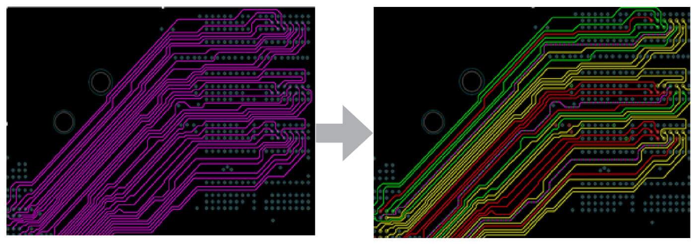
Auto-interactive routing technology
Decreasing pin pitches, greater numbers of large pin count devices, and the need to reduce the footprint all contribute to the increased challenges in planning and routing a dense PCB design. Additionally, as the PCB interconnect paradigm shifts to increased use of standardized source-synchronous interfaces (such as DDR3/DDR4) and serial interfaces (such as PCI Express), the number of constraints that must be adhered to increases. An example of a set of routing requirements for DDR3/4 interface is listed below.
Data bus requirements:
- Group and route data, data mask, and data strobe signals by byte lane
- Tightly match members inside of the byte lane
- 20 mils between members
- 5 mils differential pair phase tolerance
- It is not required to match lengths across all byte lanes. Length matching is only required within each byte lane.
-
- Byte lane members should be routed on the same layer and only use vias to escape from surface mount devices so routing can be done on an internal layer
- Should be matched within +/- 10 mils
- Routing on the same layer is not required but referencing the same plane layer is preferred
- If vias are required for multilayer routing, use the same number of vias (via matching) between each of the members
-
- Signal ended impedance target: 50 – 60Ohms
- Differential pair impedance target: 100 – 120Ohms
- All routing should be routed close to and have a solid reference plane to provide a low-impedance path for return currents
- To avoid any possible crosstalk between layers, develop a stack-up to utilize strip-line construction (reference plane above and below signal layer) instead of dual strip-line construction (two signal layers between reference planes)
Address / command / control bus requirements:
Memory interface general requirements:
Traditional automatic routers have been unable to route such dense PCBs with high-speed interfaces that require strict adherence to constraints (often derived through simulation for optimum performance on the PCB).
To reduce the time to design such boards, you should do auto-interactive routing to not only capture, but adhere to, routing intent for dense designs with highly constrained, standards-based interfaces. After capturing design intent, use feedback from the tools on such planning to adjust your routing approach.
Accelerated timing closure
As the data rates increase and supply voltages decrease in today’s advanced interfaces, PCB designers spend more time to ensure signals in an interface meet timing requirements. With increasing density on PCBs, the effort to get to timing closure—ensuring all signals meet timing requirements—can increase significantly.
To meet this increasingly complex challenge, you need an environment that allows you to graphically see real-time delay and phase information directly on the routing canvas – timing vision. Traditionally, evaluating current status of timing/length of a routed interface requires numerous trips to the constraint manager and as well as reviews of other current properties. What would be helpful here is a system to evaluate complex timing constraints and interdependencies amongst signals that show the current status of a set of routed signals—a DDRx byte lane or a complete DDRx interface. Ideally, you’d have information that defines the delay problem in the simplest terms possible.
Additionally, you need a way to leverage the feedback from the system to tune differential pairs and meet timing constraints on byte lanes as well as control and address bits, preferably in a way that reduces the manual one through tuning and adjusting. Ideally, you’d drive the strategy and execution, but have the computer do the bulk of the work to meet complex timing constraints. Such an auto-interactive strategy can allow you to tune advanced interfaces like DDRx in significantly less time compared to using traditional, more manual methods.
Multi-core CPUs or multi-CPU machines
Most personal computers these days come with dual cores. Engineering workstations tend to have more cores in one CPU. Server farms have been around for quite a while where many machines are linked in a network for compute-intensive tasks. In either case, there are several applications that can benefit from leveraging multiple CPUs—whether they are housed inside one computer or in multiple computers. These applications include:
- Solution space exploration (multiple concurrent simulations) for signal integrity analysis of digital signals
- Parametric Monte Carlo analysis for analog signals
- Batch design rules check
Predictable and reliable release schedule
Having a predictable and reliable new release schedule from your vendor allows you to plan adoption of such releases based on the value of the improvements promised. Migrating to a new release can be time-consuming, especially if you leveraged the ability to extend the base tools either through in-house developed extensions or by using thirdparty tools. An open architecture software platform that works in conjunction with third parties works best to quickly adopt new releases that have productivity, ease of use, and other critical capabilities implemented.
Divide and conquer II—outsourcing
Over the years, many companies have outsourced PCB layout partially or completely to service bureaus. Many larger global companies have opened design centers in low-cost geographies like India and China. Such companies hope to get two days’ work done in one due to time differences.
Outsourcing opens up a new set of collaboration challenges for companies. In such cases communicating complete design intent is necessary. Complete design intent implies not just traditional connectivity (parts and how they are connected) but also the constraints that these parts and signals need to adhere to. Without communicating constraints, the design cycle becomes long, arduous and, worse, very expensive. The whole reason for outsourcing may be a wash if constraints are not embedded in the design.
Once the layout is completed and sent back for review and approval, two approaches need to be taken. First, verify if any of the constraints were modified for any reason (compromises have to be made: which ones were made and are you ok with it?). Second, do post-layout verification to ensure that the realized physical implementation will work within the boundaries that are acceptable to you.
Use an open architecture
An open architecture offers freedom to choose third-party tools. All vendors will claim to have an open architecture. Often you don’t find out how open the architecture is until it is too late. There are two ways that an open architecture helps shorten the design cycle.
The first is easy access to your design data for internal consumption or for use with third-party tools. Is your design data stored in a binary or an ASCII database? Is there a way for you to extract the information easily from the binary format without having to write any software? How easy is it for third parties to integrate their tools to your design data in the primary vendor’s format?
Having a way to extract the information you need for internal use—documentation, reports, etc.—can be very helpful and can shorten the time it takes on each project significantly. Many tools offer report generation, some are customizable. Being able to create your own quickly as the need arises helps you focus on your project/design instead of struggling with the tools and tool vendors.
The second way that an open architecture can shorten the design cycle is through tool extensibility for homegrown extensions. Does the tool allow you to customize the presentation layer (GUI, menus, etc.)? Does it allow you to add-in your extensions, whether they be for report generation or for a more serious application to fill in the gap while the vendor is catching up to your need? Being able to extend the system is important. In addition, the support for such extensions should not be consistent from release to release for 5-10-12 years. Such extensions should work with all the vendors’ tools—i.e. not have discontinuity as you move up to working with advanced designs, projects with advanced tools.
Summary
In today’s environment, with increasing design complexity and continuous pressure to reduce the time to author and implement a design, you need to deploy all possible techniques and tricks to build a differentiated product quickly. At a minimum, you need to use a constraint-driven design flow in an open environment that avoids unnecessary design iterations or recreation of schematics, and allows teams to work effectively. New innovations like multi-style design authoring, global planning and routing, and FPGA-PCB co-design enable teams to create differentiated products much faster than possible with traditional approaches. Users of these technologies have reported design cycle reductions of up to 40%.