As high-speed connectors become more prevalent in various applications, PCB design teams face the challenge of optimizing the interface between high-speed connectors and PCBs with varying stack-ups and route densities, which can create crosstalk on highspeed signals. To succeed, design teams need to address this problem in its entirety, using highly accurate 3D finite element method (FEM) field solvers. The complexity of these designs requires speed, capacity, and efficient memory consumption that has not traditionally been available to users of 3D FEM tools. This application note presents an innovative workflow using Cadence® Allegro® PCB Designer and Cadence Clarity™ 3D Solver that streamlines the engineering time and effort required to address the challenges of optimizing high-speed connector interfaces within PCBs.
Design Overview
As high-speed connectors become more prevalent in various applications, PCB design teams face the challenge of optimizing the interface between high-speed connectors and PCBs with varying stack-ups and route densities, which can create crosstalk on highspeed signals. To succeed, design teams need to address this problem in its entirety, using highly accurate 3D finite element method (FEM) field solvers. The complexity of these designs requires speed, capacity, and efficient memory consumption that has not traditionally been available to users of 3D FEM tools. This application note presents an innovative workflow using Cadence® Allegro® PCB Designer and Cadence Clarity™ 3D Solver that streamlines the engineering time and effort required to address the challenges of optimizing high-speed connector interfaces within PCBs.
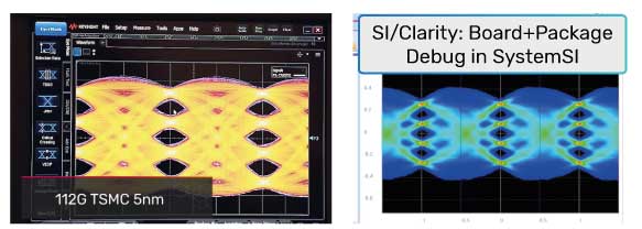
Cadence provides system-on-chip (SoC) designers with reliable high-speed connector intellectual property (IP), including robust IBIS-AMI models. The best-in-class IC package design methodology offers fast and accurate interconnect extraction using interconnect model extraction (IME) directly from Allegro Package Designer plus. The Cadence integrated PCB design and analysis solution supports optimizing PCB/connector transitions with the Clarity 3D Solver, as Figure 1 shows.
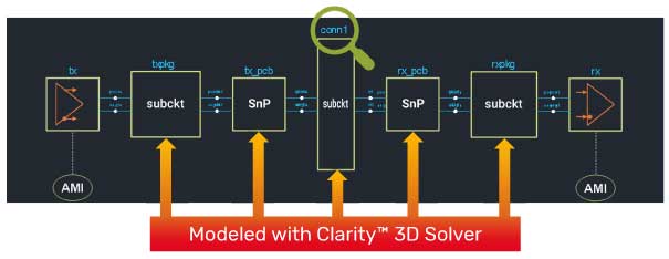
Cadence also provides high-speed connector signoff with system-level signal integrity (SI) analysis using Cadence Sigrity™ SystemSI (Figure 2).
The advantages of this flow are trusted 3D simulation accuracy, the capacity and speed to accelerate interconnect modeling, 3D FEM analysis of merged connectors (mechanical) and PCBs (electrical), protected connector vendor IP through encryption, and a reduction in error-prone re-drawing of 3D FEM optimized structures by PCB design teams through eXML back-annotation.
Merging the PCB and Connector
The default design flow typically used to merge the PCB and connector is performed by cascading the S-parameter from the connector with the S-parameter of the PCB (Figure 3).
A more desirable flow is to merge the PCB structure and connector structure and create a single model, as Figure 4 shows.
To create the desired model, the SI engineer must have a detailed mechanical model for the connector and the PCB, which can be a problem, as connector companies do not typically release the details of their mechanical design. Consequently, the systems company needs to model the PCB + connector to optimize the transition between the connector and PCB.
In the new Cadence flow, the connector company provides a detailed connector model in an encrypted format supported by the Clarity 3D Solver. The connector company releases no unnecessary connector details. Clarity 3D Solver customers can merge the PCB and the connector in the Clarity 3D workbench and accurately model and optimize the interface between the PCB and connector. The speed and capacity of the Clarity 3D solver help complete this process without cutting the merged design into smaller pieces, thus saving engineering time and reducing the risk of human error.
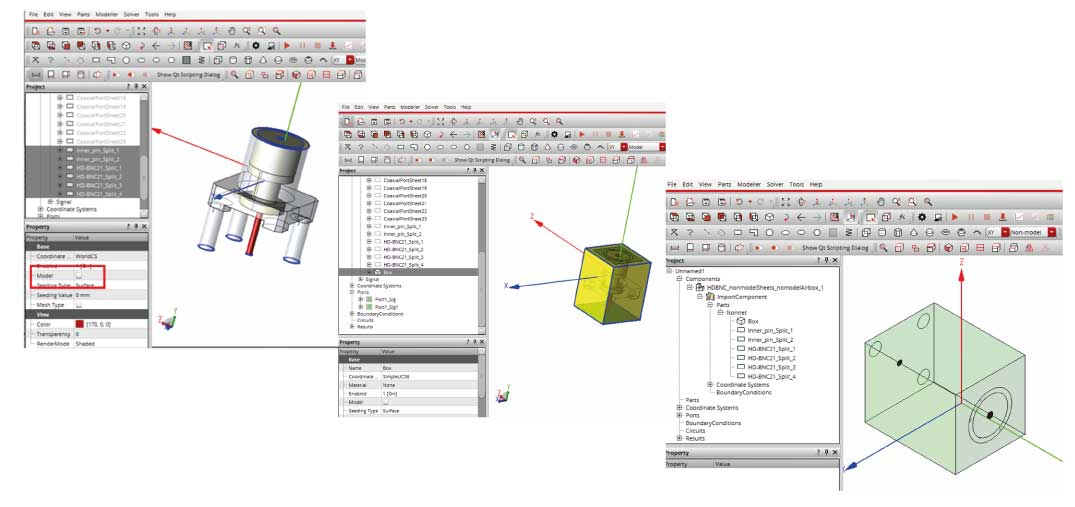
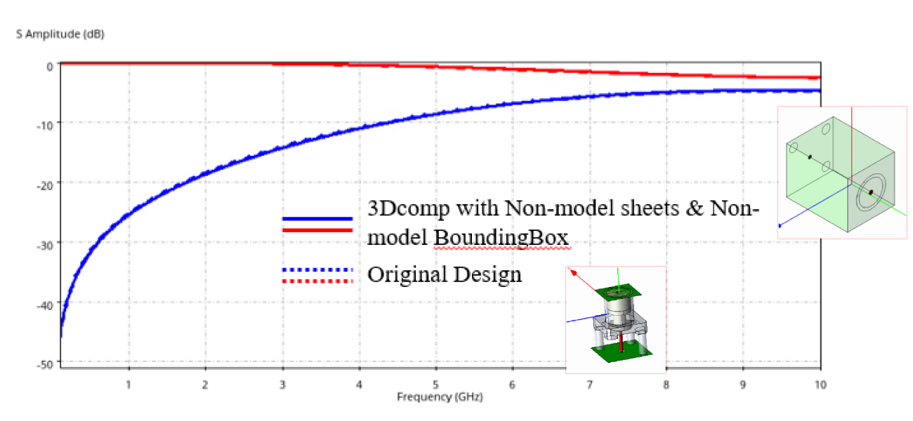
Figure 5 provides an example of the encryption process using a Cadence solution called 3D components. 3D components enable designers to create an encrypted model and show the consumer the outer portion of the design without revealing the underlying proprietary IP. In Figure 5, the left side highlights the menu that generates and exports a 3D component. The small box on the right shows the 3D connector component in full detail. The small box below shows the resultant IP-protected equivalent model with only port location and rough footprint outline.
A 3D component can be shared once it is encrypted. The receiver of the protected IP cannot see the inner workings of the components, as Figure 1 shows. The designer has successfully hidden the components’ IP from view, guaranteeing IP protection while simultaneously enabling these customers and partners to use these components to perform their multiphysics system-level simulation without any loss of accuracy.
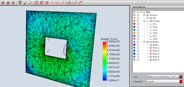
Figure 6 shows a simulation of the model, and Figure 7 shows the simulation results.
Modeling a USB-C Board and Cable
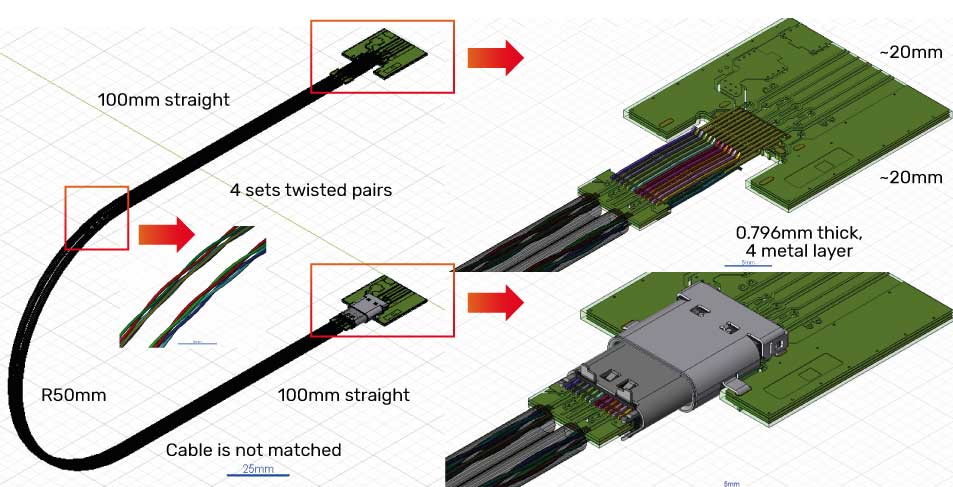
Figure 8 depicts a sample geometry for a USB-C board and cable. The PCB, USB-C receptacle, and plug are courtesy of Würth Elektronik GmbH & Co.
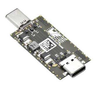
The filter stick in Figure 9 is a USB 3.1 type C 100W EMC, also courtesy of Würth Elektronik. The PCB layout STEP file for the USB-C receptacle and plugs, as well as the electrical models for the common mode choke, etc., are publicly downloadable.
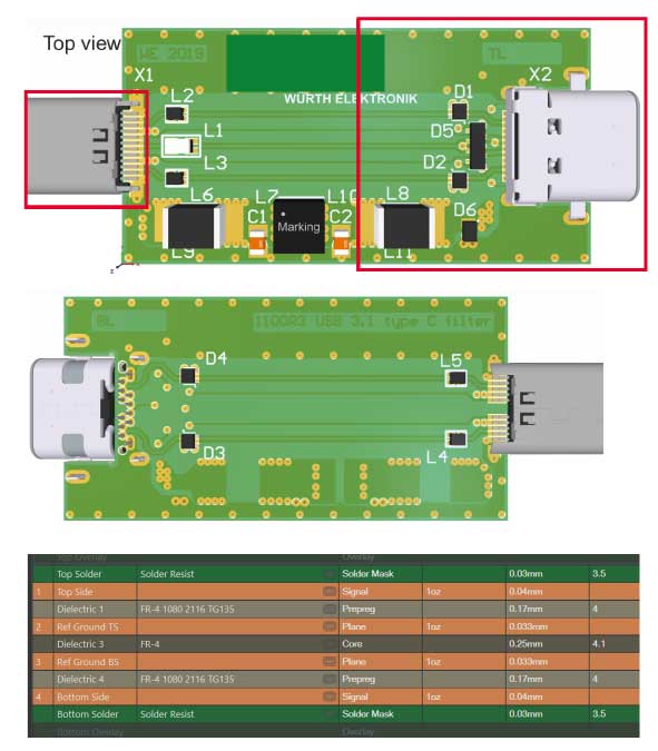
Figure 10 provides the details of the original PCB, including the top view, bottom view, and stackup.
The sections in the top view outlined in red are cut and inserted into the receptacle using the Clarity 3D workbench (Figure 11).
Connector Details
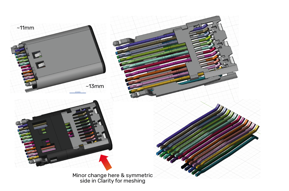
Figure 12 provides details of the USB-C connector plug. The red arrow at the bottom of the lower left figure indicates where a minor change was made to the part and the symmetric side in the Clarity 3D Solver for meshing. The top left image is the top of the plug; the lower left is the bottom. The top and lower right images show the inside of the plug.
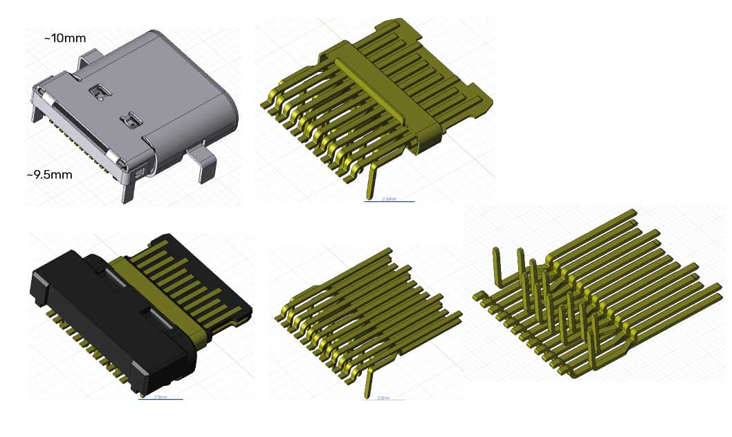
Figure 13 shows the details of the connector receptacle.
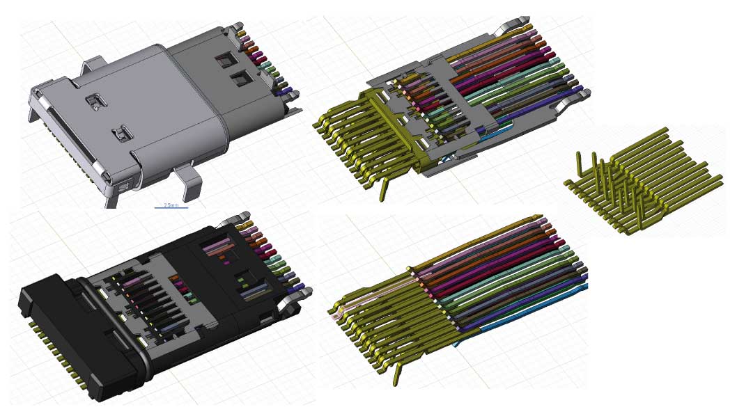
Finally, Figure 14 shows the details of the connector plug inserted into the receptacle.
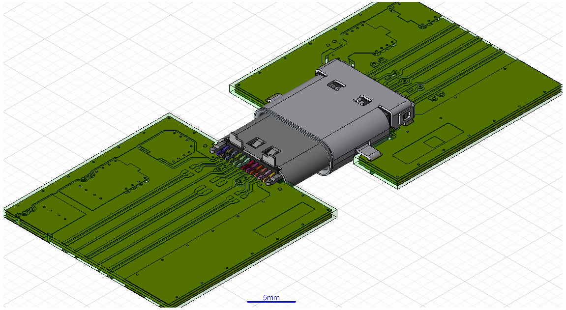
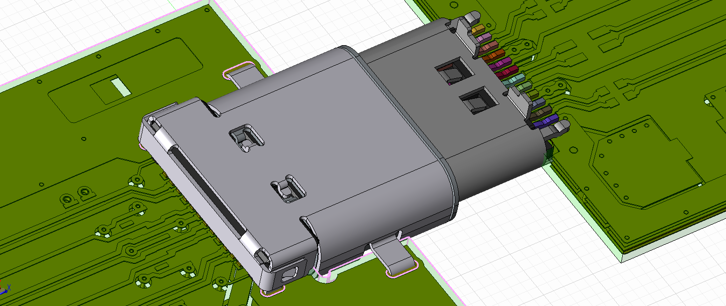
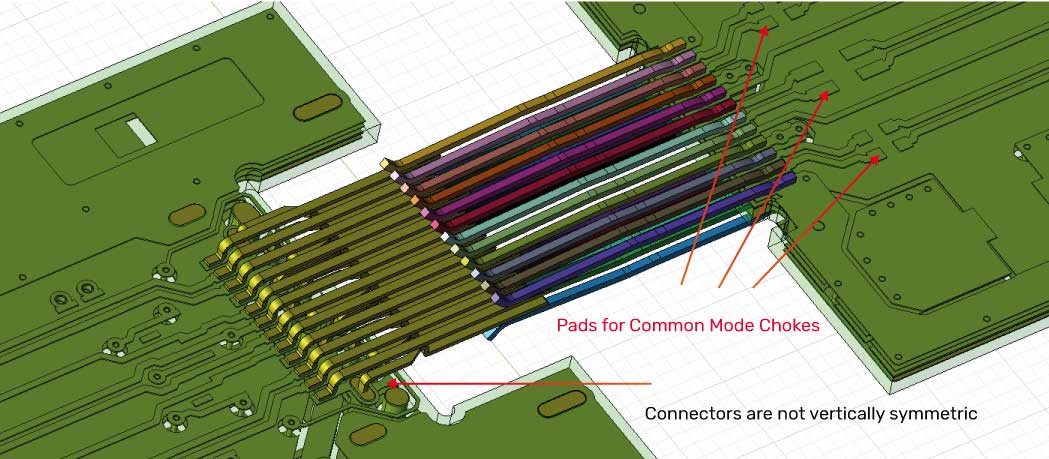
Figure 15 shows the connectors and PCB assembly layout in the Clarity 3D workbench, and Figure 16 shows a view of the connector assembly with the shield and insulator hidden.
The following should be considered for EM modeling of the connector. Several solution methods could be selected, including divide and conquer and a cascade of S-parameters. However, there is no easy way to divide and conquer. Another choice is to decide how to divide the geometry, where to define the ports, and what port types should be used.
The connectors can’t be modeled in isolation because there is no good ground reference for ports on the connector pins. In addition, using waveports to model the twisted pair cable might not be accurate as the cross-section solver captures the eigenmodes of straight cables.
It would be desirable to have a full model that includes the PCB, connectors, and cable, which can be accomplished using the Clarity 3D workbench.
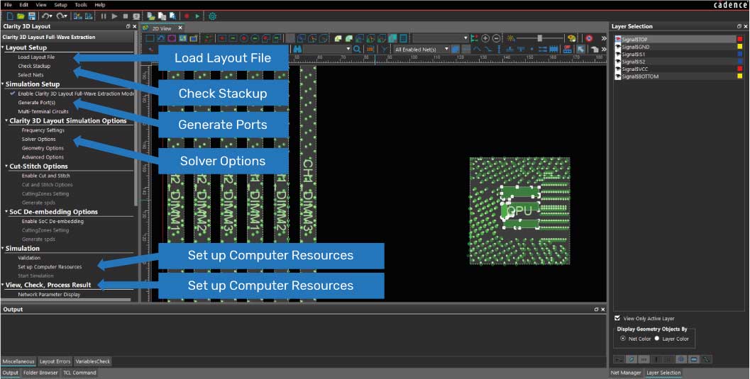
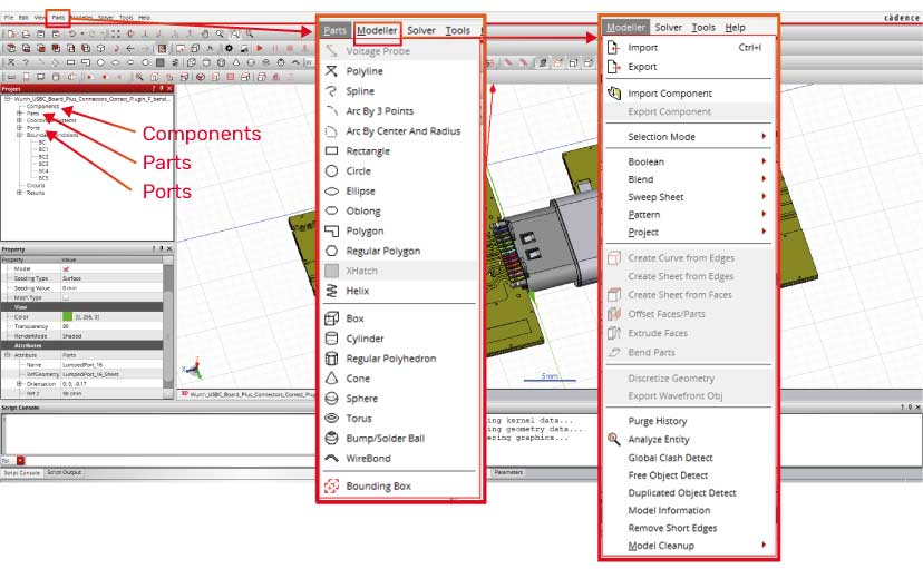
Figure 17 is a screenshot of the Clarity 3D layout user interface showing the various capabilities of the tool, and Figure 18 is the user interface of the Clarity 3D workbench.
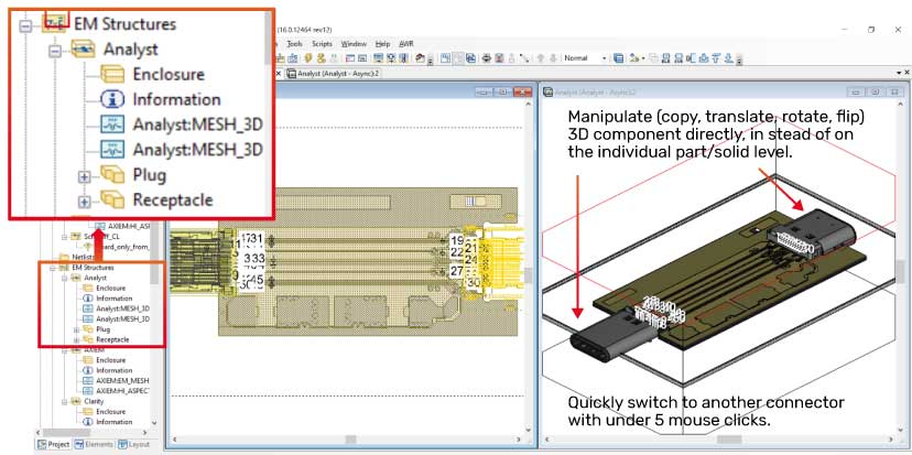
One key feature of the Clarity 3D Solver is its ability to perform hierarchical design to directly manipulate (copy, translate, rotate, flip) 3D components instead of on the individual part/solid level (red arrows in Figure 19). The designer can quickly switch to another connector with less than five mouse clicks.
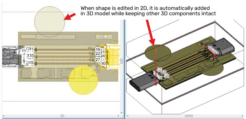
This capability is very helpful for modifying the stackup and 2D layout for 3D simulation. Figure 20 shows that when a shape is edited in 2D, the software automatically adds it to the D model while keeping the other 3D components intact.
Figure 21 shows before and after images of the connector pins being bent using the Clarity 3D Solver for 3D editing.
Clarity 3D Simulation Flow
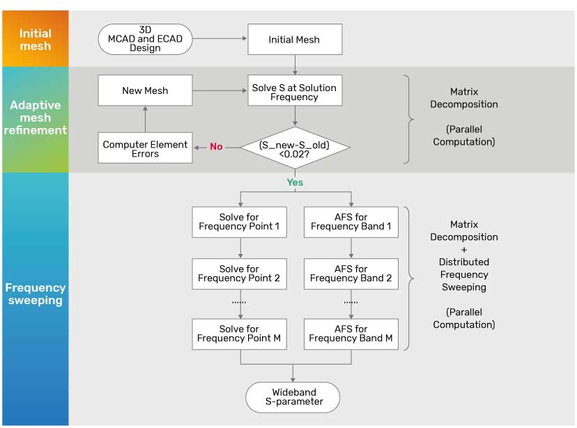
Figure 22 shows a map of the Clarity 3D Solver simulation flow.
Figure 23 is the Clarity mesh for the board only on the left and the board and connectors (no cable) with 50 ports on the right.
Figure 24 provides a close-up of the connectors on the left and the inside of the connectors on the right.
Figure 25 shows the full structure of the Clarity mesh, with the covers removed on the right.
Figure 26 is the full structure Clarity mesh twisted pair part (left) and the bent segment of twisted pairs (right).
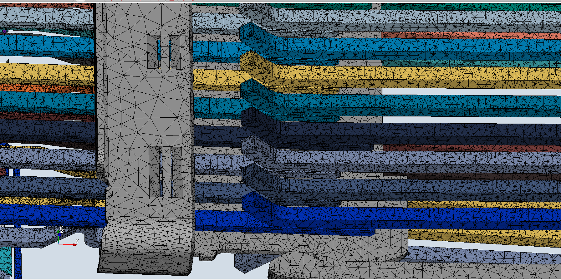
Figure 27 is the full structure of the Clarity mesh, showing the contact area of the connector pins.
Figure 28 shows the full structure field distribution (mag real part of E, p1 excited) on the left and the full structure of the field plus mesh (mag real part of E, p1 excited) on the right.
Simulation Results
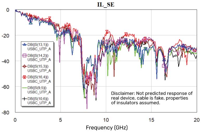
The following five images give the Clarity EM simulation results for the USB-C connector. Figure 29 is the insertion loss, single-ended, of the full structure. (Disclaimer: this is not the predicted response of a real device as the cable is not real, and the properties of the insulators are assumed).
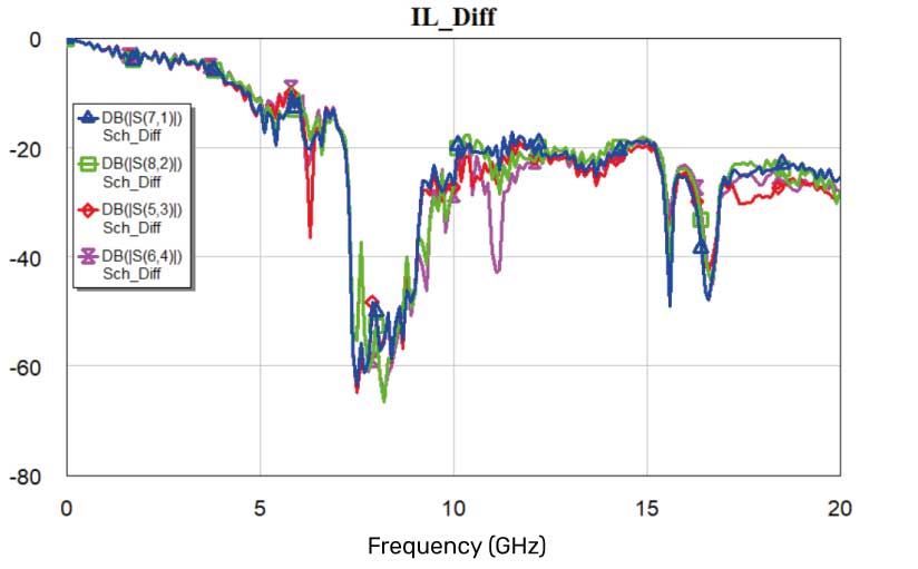
Figure 30 shows S-parameters and passivity measurement from several ports.
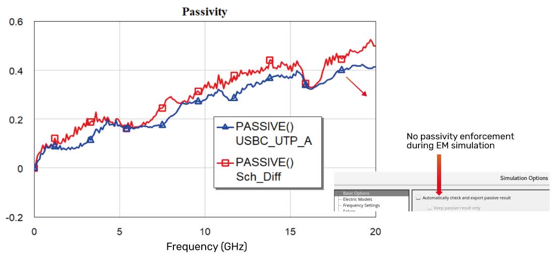
Figure 31 is the passivity measurement of several ports within the full structure. Passivity enforcement was not selected during the EM simulation.
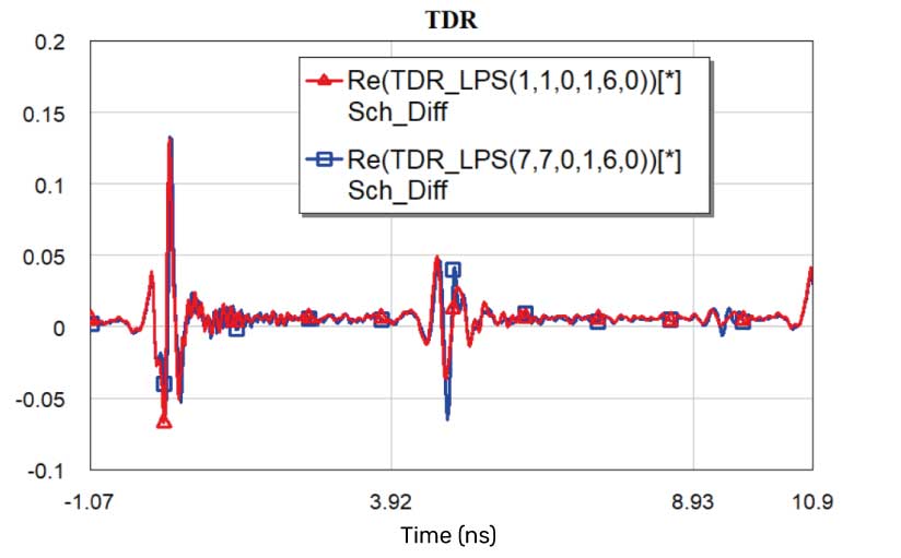
Figure 32 shows the time-domain reflectometry (TDR) measurement of two ports.
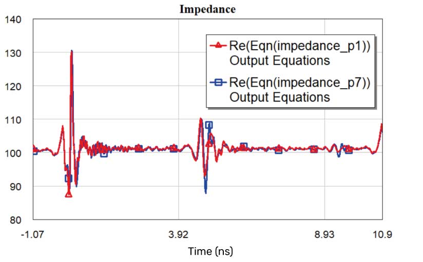
Finally, Figure 33 shows the impedance of two ports, as seen in the TDR.
Conclusion
The complexity of high-speed connector connector interface designs requires speed, capacity, and efficient memory consumption not available in many 3D FEM tools. This application note has described a unique workflow using Cadence Allegro PCB Designer and Cadence Clarity 3D Solver that overcomes the challenges of optimizing high-speed connector interfaces within PCBs by enabling designers to merge the PCB structure and connector structure and create a single model that can be efficiently and accurately simulated.
Learn more about Cadence Technologies
Cadence® Clarity™ 3D Solver
Cadence Clarity 3D Solver is a 3D electromagnetic (EM) simulation software tool for designing critical interconnects for PCBs, IC packages, and system on IC (SoIC) designs.
Cadence® Allegro® PCB Designer
Cadence® Allegro® PCB Designer helps bring your innovative and bleeding-edge designs to life. The constraint-driven environment provides real-time visual feedback and ensures the functionality and manufacturability of your PCBs while allowing you to keep designing.

