

3rd Gen AMD EPYC with V-Cache Technology Powers Cadence Computational Software
Cadence and AMD collaborate to enable engineers to create the most innovative products of tomorrow.
High-performance computing (HPC) refers to the ability of a system to perform highly complex calculations and process data at breakneck speeds.
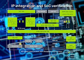
A high-performance infrastructure to handle high computing is necessary. With increasing complexity and more functionality over the chip, designers building system-on-chips (SoCs) for HPC need a combination of high-performance and low-latency IP solutions that improve total system throughput, reduce design risk in advanced nodes, and accelerate time-to-market. You need purpose-built silicon to accomplish particular objectives with maximum efficiency.
Companies designing high-performance, energy-efficient custom silicon solutions for HPC applications need purpose-built chips. The demand for purpose-built SoCs is further increasing with the massive increases in compute performance and interconnect speeds.
HPC is crucial because many computational tasks can't be performed without it — at least not in a reasonable amount of time. HPC helps solve large, complex problems in less time and at less cost than traditional computing.
You can think of each computer as a knowledgeable person who loves jigsaw puzzles. Suppose you give them a 1,000-piece jigsaw puzzle and they piece it together in an hour. That's fast.
However, what if you needed to solve an 8,000-piece jigsaw puzzle in an hour? It would make more sense for the jigsaw giant to call up seven buddies so they could tackle the job together.
The basic architecture of HPC is very similar to a regular computer connected to a network. There are three primary components:
The servers are grouped into clusters where they combine forces, sending and receiving data to and from the storage units through the network.
All of these components work together to accomplish tasks. The key is that each element needs to be fast enough to avoid latency that could result in processing delays.
Artificial intelligence (AI) applications such as autonomous driving, facial recognition, and genomics generate vast amounts of data and drive demand for purpose-built SoCs for HPC systems.
The purpose-built SoCs for HPC applications can provide a robust, highly scalable solution with tremendous improvements in memory bandwidth enabled by advanced interconnects and innovative packaging technologies (2.5D/3D)
Recent chip developments driven by OEMs have demonstrated impressive performance with a highly automated driving platform. Instead of using existing chips on the market, a purpose-built SoC tailored to the system requirements can make a huge difference.
A high-performance purpose-built SoC or system-in-package (SiP) is needed to meet demanding HPC requirements such as High Bandwidth Memory (HBM2E) IP subsystem, die-to-die (D2D) interconnect, and HBM memory die into a single advanced package.
With the incorporation of purpose-built silicon, organizations can further enhance how they leverage HPC, harnessing the horsepower of HPC to tackle specific business objectives. For example, instead of presuming a high-performance computing system will "be enough" to handle your workloads, you can have chips custom-designed to provide the processing power specific jobs need.
For instance, using an on-chip environment instead of traditional software for intelligent management in all-flash storage systems can help customers to achieve high-performance with reduced latency.
Of course, all-flash storage is a relatively small niche. However, the same general approach can put purpose-built silicon to work for an unlimited number of applications. This is where Cadence's solutions come into play.
Cadence helps customers design the chips that make HPC possible and provides several technologies that enable the horizontal scalability necessitated by hyperscale computing systems. For example, Cadence's three-dimensional integrated circuits (3D-ICs) solution is very effective for chip manufacturers as 3D-IC is ideal for an HPC system that needs to process big data because it provides more processing power while using less space.
If you picture a typical circuit board, such as one inside a PC, it consists of essential components that take up real estate on the chip, so in a traditional system, you can only fit in so many components, limiting your computing power. Cadence's 3D-IC systems take advantage of the third dimension—the vertical axis—to give you more computational power per square inch of board space. In other words, if a traditional circuit board is like a suburban block with one-story ranch homes, Cadence's solution replaces those ranches with multi-story apartment buildings.
Low latency, high bandwidth, and less data movement are the major requirements for maximizing HPC performance.
This can be taken care of by technologies such as the Cadence CXL, DDR5, PCIe, and SerDes IP. This technology supports hyperscale storage and computing by making it possible to process more data using less energy and space. This is ideal for cloud solutions that need to hyperscale in response to the high data demands of 5G networks. Therefore, Cadence provides the foundational technology to support hyperconnected lifestyles and business systems that have already begun to dominate the digital ecosystem.
To learn more about high-performance computing, connect with Cadence today. You can also check out these helpful resources: