Key Benefits
- 効率的な製品づくり
- 開発サイクルを短縮するためのコンストレイント・ドリブン PCB 設計
- システムコストと性能を最適化する協調設計と協調解析
- 製品の信頼性向上とコスト管理向けの電気的検証とサインオフ
- 製造への効率的なハンドオフによる設計とサプライチェーンのコラボレーション
効率的な製品づくりを可能にする
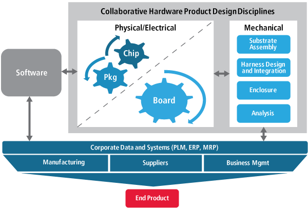
製品の作成は、チップまたはボード設計を超えており、ソフトウェアアプリケーション、メカニカルエンクロージャー、および基礎をなす電子機器を含む製品全体を考慮しています。電子製品を作成するプロセスには、作成者や実装者を超えたチームメンバー間のコラボレーション、設計プロセスの企業システムへの統合、製造パートナーとの効率的な連携が含まれます。
PCBは成功した電子製品を構築する統合点であるため、ケイデンスはAllegro® PCBおよびICパッケージ設計ツールやSigrity™ SI/PI解析ツールを使用し、製品作成ステップを実行しています。製品作成のための当社の重点分野は次の通りです:
- 設計オーサリングとコンストレイント・ドリブンPCBレイアウト、配線とチューニング
- シリコン/パッケージ、パッケージ/ボード、ボード/ボード間での協調設計と協調解析
- 機械系CAD-電気系CADボードエンクロージャー協調設計
- 省電力志向の電気的検証とサインオフ
- 製造への効率的なハンドオフによる設計とサプライチェーンのコラボレーション
関連ビデオ:
Cadence Enables Fast and Efficient Product Creation
With the Allegro constraint-driven design flow, we are now able to take a project from design to manufacturing in four to six months, depending on the complexity of the project. This represents a more than 25% improvement in productivity from our previous process.
Michael Hu, Director of Interconnect Design Group, R&D, Huawei Technologies
The AiDT feature in Allegro PCB Designer ended our frustrations over all of the time we were spending on routing and tuning. All of hours we're saving as a team [now] can be directed toward new project requests for the business.
Sky Huang, Deputy Director of Computer-Aided Engineering, Pegatron
With Allegro TimingVision, everything is right there in front of you—this simple fact allows the routing process to be sped up dramatically, from the manual routing efforts we have seen that can take up to four weeks, down to four days.
Bill Munroe, Principal PCB Designer, Cavium