- Why Most Tools Aren’t Ideal for Flat Analysis at Advanced Nodes
- Timing Analysis: Pros and Cons of a Hierarchical Methodology
- How Scope-Based Timing Analysis Improves Runtime and Capacity
- Power Integrity Analysis: Hierarchical Architectures and Massively Parallel Execution
- Achieving Faster Design Closure
- Summary
- Further Information
White Paper
Techniques to Accelerate Power and Timing Signoff of Advanced-Node SoCs
This is an all-too-familiar refrain in the electronics design world: systems on chip (SoCs) are growing increasingly complex and time-to-market windows are shrinking. This is especially true at advanced nodes. In the face of these challenges, both timing signoff and power signoff of digital designs have become increasingly time-consuming last steps toward design closure. Fortunately, new signoff technologies have emerged to alleviate the signoff bottlenecks. This paper takes a look at how novel approaches such as scope-based analysis, hierarchical architectures, and massively parallel algorithms facilitate faster timing and power signoff.
Overview
Why Most Tools Aren’t Ideal for Flat Analysis at Advanced Nodes
Complex design rules, low-power circuitry design techniques, and signal integrity issues are just a few of the advanced-node challenges impacting design closure. While timing analysis and signoff and power integrity analysis and signoff are critical to successful design closure, both of these steps can also be quite time-consuming and resource-intensive.
On the timing signoff side, determining if clocks and signals are timed correctly has traditionally called for static timing analysis tools. Depending on the design size, static timing analysis has typically been performed either flat or hierarchically. Flat analysis, where the design is flattened down to one top-level layer, yields the most accurate results, since it is completely transparent down to the logic cells. However, flat analysis requires more memory and time to run because every cell and wire in the design is analyzed. With larger designs, most of the tools on the market that perform flat analysis aren’t ideal because of their long runtimes.
For large, complex designs with hundreds of millions of instances, applying a flat methodology for power signoff also requires the right tool. Many of the power signoff tools available today are point tools that don’t provide the accuracy or ease-of-use needed to support the requirements of advanced SoCs. What’s more, many of these tools also lack an efficient means for engineers to assess the impact of power on timing closure, even though timing is most sensitive to the voltage supply (VDD), or the effective voltage supply on each instance along a timing path. Also considerations are the new challenges that advanced-node design technologies like the FinFET process and 3D-IC packaging bring to the mix.
For faster, more effective timing and power signoff, new techniques involving scope-based analysis, hierarchical architectures, and massively parallel algorithms are quickly proving their worth in resolving many of the bottlenecks. Let’s start our discussion by looking at different methodologies for timing analysis.
Timing Analysis: Pros and Cons of a Hierarchical Methodology
For timing analysis, a hierarchical design methodology allows a team of engineers to collaborate on a single chip. The team creates timing budgets throughout the design, often at the pins of the blocks. Then, team members can close timing on their blocks, independent of top-level analysis. Compared to full flat analysis, this approach is a practical way to manage the size and complexity of today’s SoCs. However, it also leaves open the possibility that some critical timing issues might be missed, particularly in paths that cross hierarchical boundaries.
There are different modeling approaches in hierarchical timing analysis that address accuracy concerns. Extracted Timing Models (ETMs) take the form of Liberty models (.lib) and use abstraction to minimize the amount of data while aiming to preserve accuracy. By replacing respective blocks in hierarchical timing analysis, ETMs can speed up analysis quite a bit and also minimize the memory footprint for full-chip analysis. Most ETMs do, however, have limitations that can impact the efficiency and even the accuracy of hierarchical analysis, including model generation, validation, and merging; signal integrity-aware ETMs, and multi-mode, multi-corner (MMMC) ETM generation.
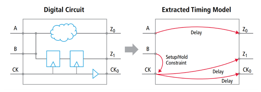
Figure 1: Extracted timing models
Another highly accurate modeling approach is the Interface Logic Model (ILM), which removes the register-toregister logic and preserves the rest of the interface logic and associated parasitic capacitance information. ILMs can provide a substantial boost in analysis speed while also reducing the memory footprint. Since they preserve the interface logic in the same exact way as the original netlist, ILMs can deliver the same timing for interface paths as can a flat analysis. The approach does, however, have limitations, including over-the-block routing, constraint mismatches, and arrival pessimism.
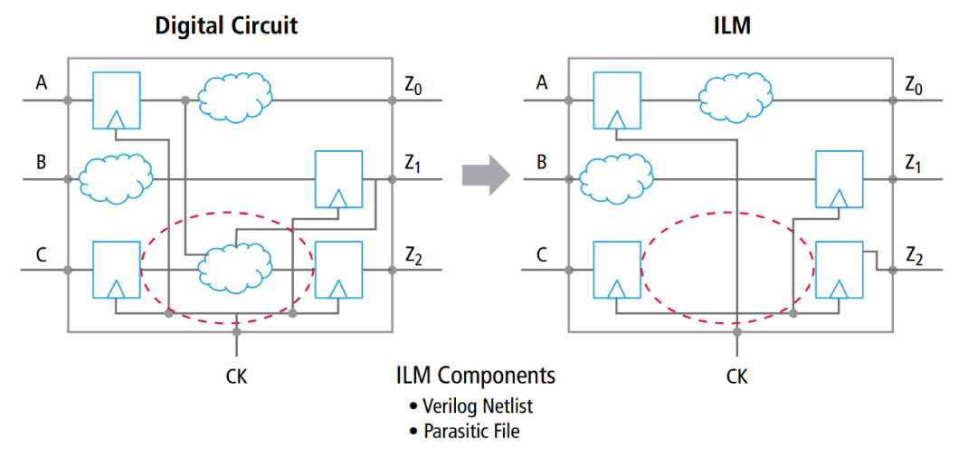
Figure 2: Interface logic model
There are tools available that attempt to resolve the limitations in ETMs and ILMs by concurrently analyzing all of the hierarchical blocks in the design. What happens here is, the block hierarchy of the design is used to create design partitions, which are then timed independently. To resolve dependencies between the partitions, constraints are asserted at the block boundaries and other data at the block boundaries are synchronized. The analysis is performed iteratively; new constraints are asserted in each analysis iteration until a designated convergence criterion is met. While this approach reduces some of the capacity limitations that full flat analysis has, it does, however, come with its own limitations.
How Scope-Based Timing Analysis Improves Runtime and Capacity
A novel new approach involving full flat distributed timing analysis along with the ability to time only the portion of the design influenced by a changed block is yielding substantial improvements in runtime and capacity. In addition, this approach—scope-based timing analysis—also maintains the high accuracy that is so critical to this step toward design closure. With this new methodology, there’s virtually no limit to the design sizes that can be analyzed flat.
Available in the Cadence Tempus Timing Signoff Solution, scope-based timing analysis lets you dynamically abstract only those portions of the design that you want to analyze. And, you can analyze the portion with full chip-level context. The way it works is, you define the change space at the level of granularity that is equal to the physical/logical block boundaries. Once the Tempus Timing Signoff Solution has the blocks or top-level scope, the solution handles the dynamic abstraction of the design and analyzes the resulting “carved out” design in a much faster manner and with a smaller memory footprint than alternative methods. In fact, the solution has demonstrated the ability to perform analysis 2X to 3X faster than traditional full flat analysis. The tool also provides a distributed processing capability, so you can run each scope-based analysis in parallel if needed.
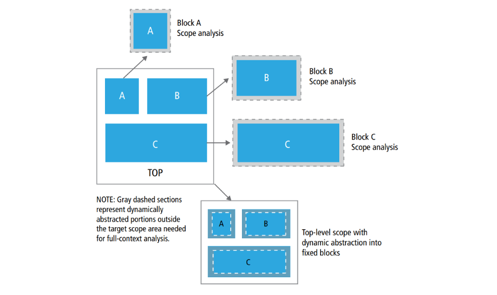
Figure 3. Scope-based timing analysis
Power Integrity Analysis: Hierarchical Architectures and Massively Parallel Execution
On the power integrity signoff side of design closure, one of the main goals is to detect “hot spots” or voltage drop (IR-drop) exceeding a threshold on the chip as early as possible to prevent degradation of chip performance. Saving valuable development costs and time calls for debugging and verifying that power and IR-drop constraints are met across today’s multi-hundred to multi-million instance designs and multiple die. Here, a hierarchical methodology combined with massively parallel algorithms and other signoff-quality algorithms is proving to be accurate, fast, and ideal for high-capacity, advanced-node SoCs. These technologies are all available in the Cadence Voltus IC Power Integrity Solution.
With a hierarchical approach, you can build a power-grid model, representing the lower level part of your design hierarchy with the power-grid information of interest. This model can be re-used on multiple instances, as “repeated blocks,” at the top level. As a result, you can run much larger design instance numbers in your analysis, compared to a flat methodology. In addition, the multi-threaded, distributed processing techniques of the Voltus IC Power Integrity Solution enable it to extend its fast performance levels across a computer network at high capacities (up to one billion instances).
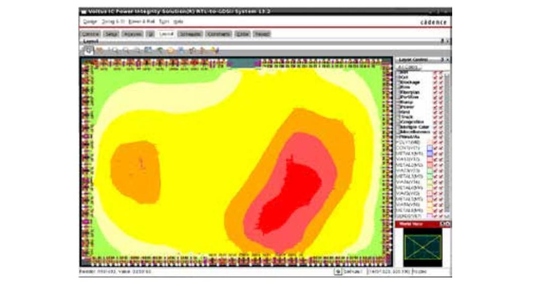
Figure 4. Detecting an IR-drop hot spot using Voltus IC Power Integrity Solution
With its massively parallel algorithms, Voltus IC Power Integrity Solution performs 10X faster than competing tools. In one user example involving an advanced-node design with several hundred million instances, the solution completed the power signoff process in 26 hours on 32 CPUs. By comparison, on an existing production flow, hierarchical static and dynamic power signoff would have taken about 10 days to complete. Accuracy is not compromised, as the solution features a SPICE-level rail matrix solver and accurate power-grid RC extraction and instance power calculation and distribution.
Achieving Faster Design Closure
While tools discussed here are speeding up both timing and power signoff, they can also contribute to a faster overall design closure process when used with complementary tools that form a complete signoff flow. This flow makes it possible to employ techniques such as early rail analysis, real-world peak power analysis, and unified electrical signoff.
Under a traditional design flow, power signoff analysis would usually happen after the design has been placed and routed. The disadvantage here is that any power integrity problems found at this stage would require either much longer to resolve or be irreparable. Since Voltus IC Power Integrity Solution is integrated with Cadence Encounter Digital Implementation System, you can consider the power-grid design at the early stage of physical implementation. This early rail analysis capability considers floorplanning information along with the size and location of the power-grid metals. So, if you have to place two function blocks together, the integration of the two tools guides you on how to best apply placement and routing on the grid. With a positive early rail analysis result, you can achieve faster convergence of power signoff and faster design closure.
Voltus IC Power Integrity Solution is also integrated with Cadence’s Palladium emulation technology. The combination of these solutions provides highly accurate IC power integrity analysis that’s driven by real-world power stimulus from the Palladium platform’s “deep cycle” Dynamic Power Analysis capability.
As noted previously, timing and voltage drop analysis are intertwined—switching times affect current draw on power rails, and power rail voltages affect cell delays. Convergence on realistic rail voltage and timing requires iterations. Voltus IC Power Integrity Solution is integrated with the Tempus Timing Signoff Solution, creating a unified power and timing analysis and closure system. The result is an iterative timing/IR-drop analysis process, with increased accuracy in static timing analysis, reduced timing pessimism, and a more realistic voltage drop across the chip.
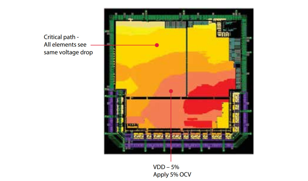
Figure 5. On-die voltage variation is traditionally margined as a constant derate in delay.
There’s also a part of this complete signoff flow that addresses system-level concerns. Namely, at the chip and PCB stages, you want to prevent thermal crashes of packages, plus any other power integrity issues. To alleviate these problems, the Voltus IC Power Integrity Solution is integrated with Cadence Allegro Sigrity technology to provide chip-package-PCB co-simulation and analysis. This integration fosters faster system-level power integrity analysis and closure.
Summary
As SoCs have grown in complexity, so too has timing and power signoff. Fortunately, there are new technologies available that are alleviating the bottlenecks in these processes. Techniques available in the Tempus Timing Signoff Solution and the Voltus IC Power Integrity Solution—including scope-based analysis, hierarchical architectures, and massively parallel algorithms—are speeding up timing and power signoff. Moreover, these solutions are part of a complete signoff flow that is accelerating design closure, helping engineers meet time-to-market goals for the complex, advanced-node SoCs at the foundation of today’s smart connected devices.
Further Information
Learn more about Tempus Timing Signoff.
Learn more about Voltus IC Power Integrity Solution.