White Paper
Overcoming Signal, Power, and Thermal Challenges Implementing GDDR6 Interfaces
Graphics processing units (GPUs) and graphics double data rate (GDDR) memory interfaces are essential to graphics cards, game consoles, high-performance computing (HPC), and machine learning applications. These interfaces enable data transfer speeds of over 665GB per second today and will continue to support well over a terabyte per second (TBps) in next-generation GDDR interfaces. Signal integrity (SI) and power integrity (PI) are becoming intertwined with the thermal issues caused by ultra-fast data transfer rates, ultra-low voltage swings, and high-density GDDR6 designs often implemented on silicon interposers. This paper describes using power-aware SI analysis and thermal-aware PI analysis as part of a system design and signoff methodology for GDDR6 designs.
Overview
Overview
GDDR is an evolving interface used for many electronic applications. It is typically used in graphic-intensive applications, such as gaming consoles and graphic cards; however today, high bandwidths have allowed GPUs to progress to other applications, enabling high-performance applications such as machine learning (ML), artificial intelligence (AI), graphics, advanced driver assistance systems (ADAS) for automobiles, and HPC. As more companies invest in the heterogeneous integration of semiconductors to address these next-generation applications featuring GDDR6 interfaces, they are looking to partner with intellectual property (IP) providers for the GDDR6 memory controller.
Cadence is uniquely positioned as an IP provider for GDDR6 and an EDA tool provider. The Cadence IP group utilizes the complete EDA tool suite to create test chips, packages, and PCBs. Regardless of the source of the GDDR6 design IP, system integrators can have confidence in the Cadence holistic design and analysis solution, knowing that the technology has been used for actual design work by the same company that provides the tools. The solution includes design and simulation tools for the chip and the interconnect in the interposer, IC package, and PCB. Tools within the solution include the Cadence Clarity 3D Solver electromagnetic (EM) simulator, Cadence Celsius Thermal Solver, and Cadence Sigrity X SI/PI technologies to simulate and sign off on Joint Electron Device Engineering Council (JEDEC) specifications, so that GDDR6 implementations perform to industry standard requirements at an optimized cost.
Key Issues to Consider in GDDR6 Design
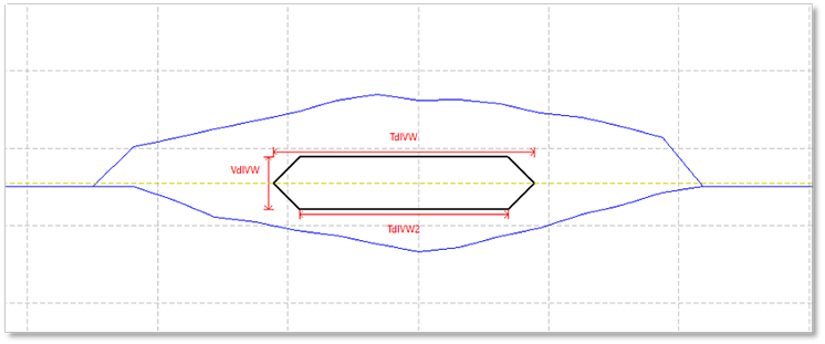
With the evolution of DDR interfaces, setup and hold checks are no longer the sole approach to checking interface timing compliance. While still part of the process, timing is now managed through various mask requirements. Figure 1 shows a mask used for the data bus. Multiple mask checks examine the relationship between address, control, and data, and the various strobes/clocks used to latch the signals both at the rising and falling edge of the clock/strobe.
One of the changes with GDDR6 compared to previous versions of GDDR is a data inversion for both the data bus (DBI) and command/address bit inversion (CABI), which reduces the number of signals that need to switch simultaneously. This reduces simultaneous switching noise (SSN), which in turn reduces bit errors, ensuring that GDDR6 interfaces achieve the required bit error rate (BER). The accurate simulation of the latest GDDR data transfer speeds requires that both the controller and memory devices support the modeling of feed-forward equalization (FFE), continuous time linear equalizer (CTLE), and decision feedback equalization (DFE) with input/output buffer information specification (IBIS) algorithmic modeling interface (AMI) models.
In-Design Analysis
GDDR6 design requires an exhaustive signoff process, but design teams can advance through the signoff stage faster by using in-design workflows early in the design process. In-design analysis complements a constraint-driven flow. Constraints provide rules that designers must follow, but in-design analysis provides simulation engines to designers while they are laying out their design. This enables design teams to find problems earlier in the design cycle, which means less time spent in the exhaustive signoff analysis stage.
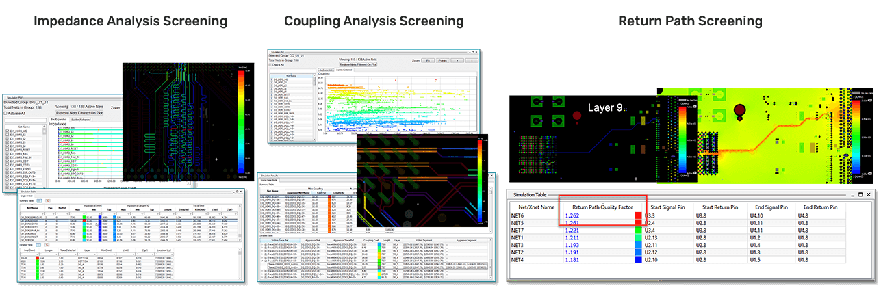
Designers of memory interfaces such as GDDR6 must focus on both impedance discontinuities and return path quality. Figure 2 illustrates the electrical rule check (ERC) screening technologies that can be performed during PCB design. Impedance analysis helps designers identify outliers, such as traces routed over splits in power/ground planes (left). They can also analyze coupling, providing early insight into potential crosstalk problems without using IBIS models (center). Finally, designers can analyze the return path to uncover nets with possible return path problems using the return path quality factor as a figure of merit. Selected signals highlight the return current flow on the planes so that they can visualize and change the return path quality directly within the PCB design environment (right).
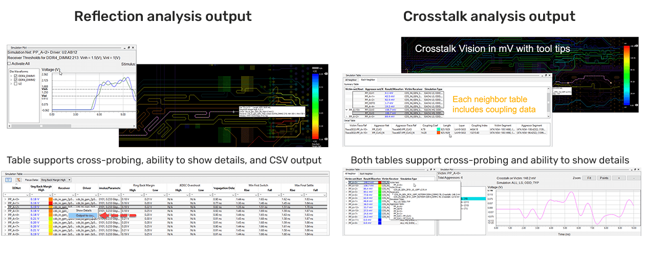
For a more sophisticated analysis. designers can call on reflection and crosstalk workflows that enable viewing time-domain waveforms. Simulation is enabled by industry-standard IBIS models assigned to the components in the implementation environment. With those IBIS models in place to model the I/O, reflection and crosstalk analyses reveal the overall signal quality (Figure 3).
SI Testbench for GDDR6 Memory Interface
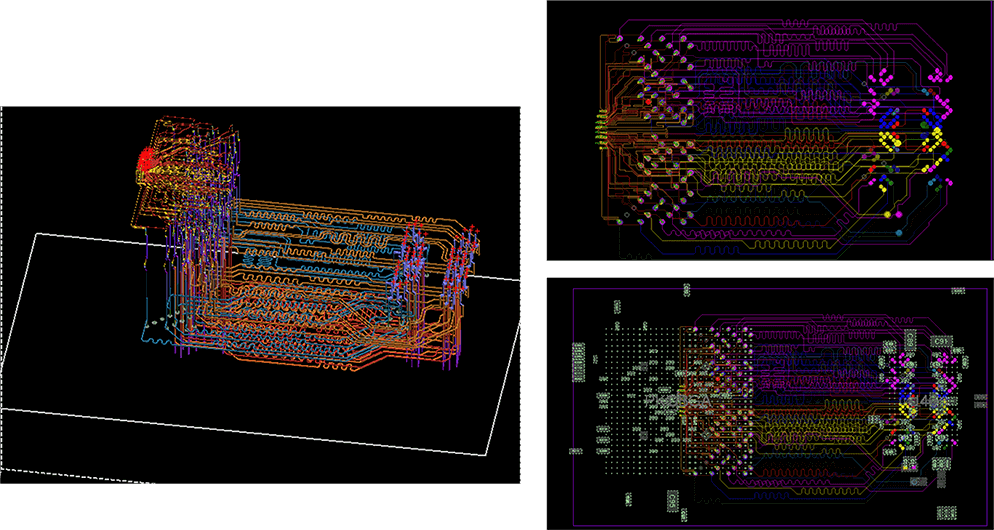
One of the key steps in GDDR6 design is extracting the interconnect from the PCB and IC package. There are different approaches to modeling system interconnect using Cadence tools: the Sigrity X PowerSI hybrid solver, the full-wave 3D finite element method (FEM) Clarity 3D Solver, or a combination called the “cut-and-stitch flow.” Companies with access to both PCB and IC package design data can merge the PCB and the package to perform an extraction that will include the coupling between the IC package and PCB (Figure 4).
PCB design teams without access to the package design should request their semiconductor vendors for package models for the memory controller and the memory, which can be cascaded with the extracted PCB model to perform system analysis design.
If the design is implemented using the Cadence PCB or package design tools, the design data, including the stackup and material properties, will be automatically read into the extraction tool without requiring manual input. Designs from non-Cadence design tools are read in through IPC-2581 or ODB++ manufacturing file formats.
The Clarity 3D Solver is a robust FEM solver that offers parallelization and distributed computing technologies that allow for full-wave 3D extraction of large, complex designs done in a fraction of the time as legacy FEM tools. The Sigrity X PowerSI tool also incorporates distributed computing technologies to quickly extract S-parameters using a hybrid solver. In this GDDR6 example, PowerSI technology provided a full model in 15 minutes while the Clarity 3D Solver solved the same problem with a full 3D FEM approach in 1.5 days using 64 cores. The cut-and-stitch methodology blended the two approaches for improved accuracy over the hybrid solver alone, providing results in hours.
Which extraction technology to use and when? As a first step, designers can use PowerSI hybrid extraction to obtain a quick extraction for a first pass look at the S-parameters. They can examine the insertion loss, return loss, and fundamental frequencies and determine if the layout needs modifications. For signoff, they should use Clarity 3D FEM extraction. Between initial modeling with PowerSI and final signoff, designers can use the cut-and-stitch flow to focus on areas of interest around the interface and assign extraction techniques to each area. They can assign areas with vias, via-stubs, non-uniform return paths, etc. To the Clarity 3D Solver, and assign areas with long transmission lines that are well behaved and have a uniform return path to the hybrid solver. As the design matures, they can combine these two solvers to provide fast and reasonably accurate results in a fraction of the time of a full 3D FEM extraction and serve as a balance between accuracy and extraction time.
The scalability of the Clarity 3D Solver provides an alternative way to accelerate the signoff process. With additional CPU cores made available, one could accelerate the GDDR6 example that was completed in 1.5 days. Doubling the number of compute cores will typically cut the simulation time nearly in half. In addition, the process is very memory efficient—32-core machines with 256GB of memory are more than sufficient to complete the task. If there is a lack of compute power on the premises, designers can use the Clarity 3D Solver Cloud solution. With Clarity 3D Solver Cloud, all the setup is done on the local machine, and the simulation is sent to a secure AWS cloud. The results return to the on-premise machine just as if the simulation had been run locally or on an on-premises server farm.
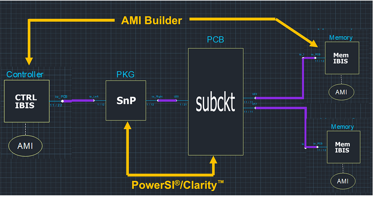
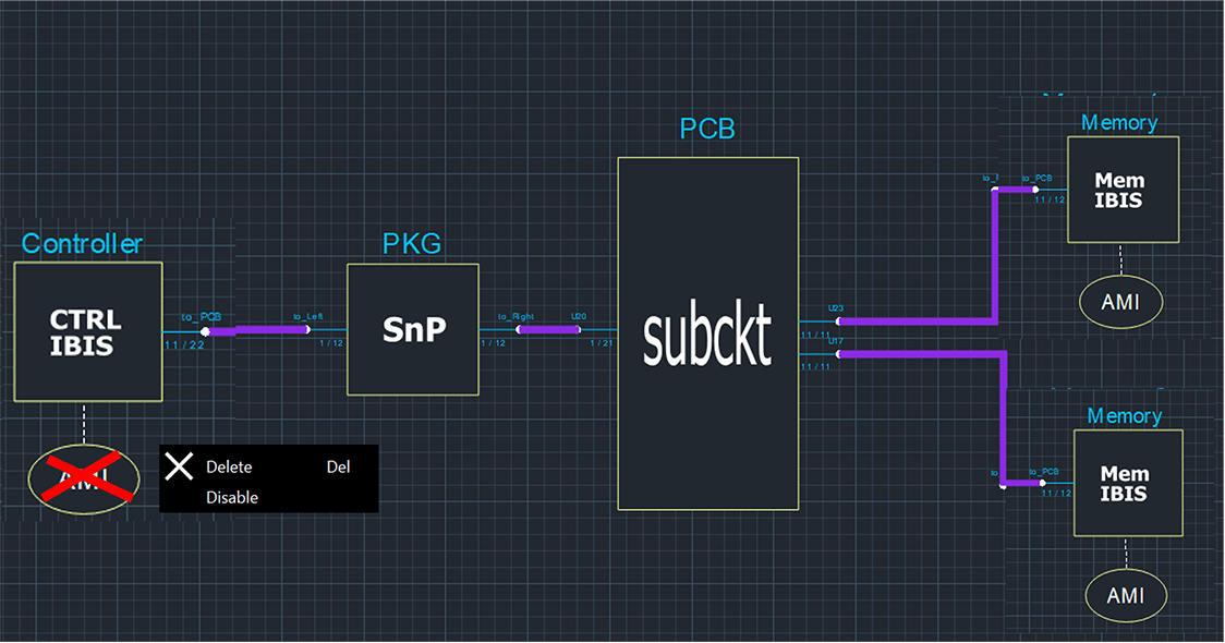
Parallel bus topology creation
After extraction, the designers create the topology using the topology workbench within the Sigrity X SystemSI parallel bus analysis (PBA) tool (Figure 5). This GDDR6 interface shows the block-based topology where the designer places blocks in the different portions of the interface. Figure 5 shows an onboard memory example with IBIS models for the controller and two memory devices. Between the IBIS models are separate interconnect models for the IC package and the PCB. As mentioned above, an alternative approach would be to combine the package and PCB into a single interconnect model to capture the EM impact between the IC package and PCB. Note that IBIS AMI bubbles have been attached to the IBIS models. All the blocks are connected—the purple connectors represent multiple connections between the blocks (only one line is visible, but there are multiple connections). Once the connections are made, the analysis can be started.
Traditionally, channel simulations have been done on serial links, and more specifically, with differential pairs. Cadence has developed and patented channel simulation on single-ended signals, enabling designers to simulate the millions of bits required for interfaces such as the GDDR6 that include both SSN and crosstalk effects. A correlation of the circuit simulation with the channel simulation can easily be performed within the workflow, using the default options or rising ramp responses, falling ramp responses, or both rising and falling responses. The workflow steps for this flow are unique for the signoff of high-speed memory interfaces.
The IBIS AMI portion of the channel simulation requires models that ideally will come from the component vendor. When the vendor cannot supply an IBIS-AMI model, a wizard-based workflow allows you to create an IBIS-AMI model based on the component specification.
All the steps in the parallel bus SystemSI PBA environment are workflow-based. There are workflows for setup, simulation, and evaluating the results. The workflows support different types of analysis, including circuit simulation and channel simulation, and the ability to incorporate those with a bus simulation. Lastly, there is an intuitive simulation parameter setup for stimulus definition and model selection.
Workflow Steps
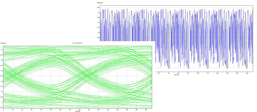
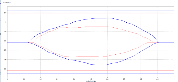
The first step in the workflow is to run a circuit simulation to examine the waveform quality and ensure the eye diagram has no issues (Figure 6).
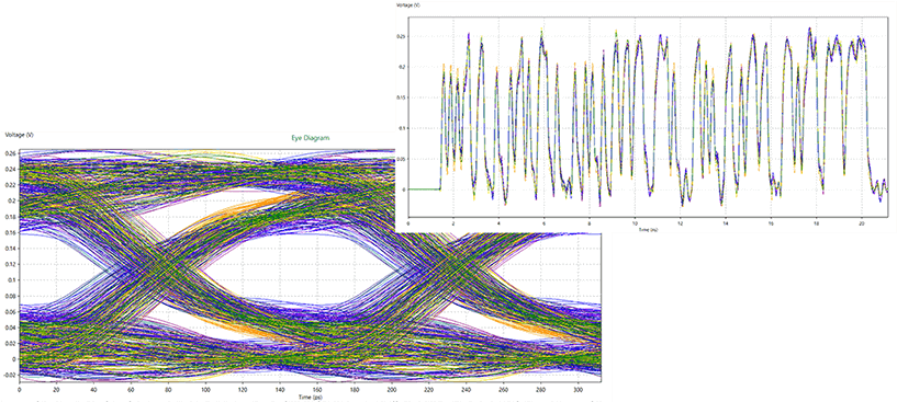
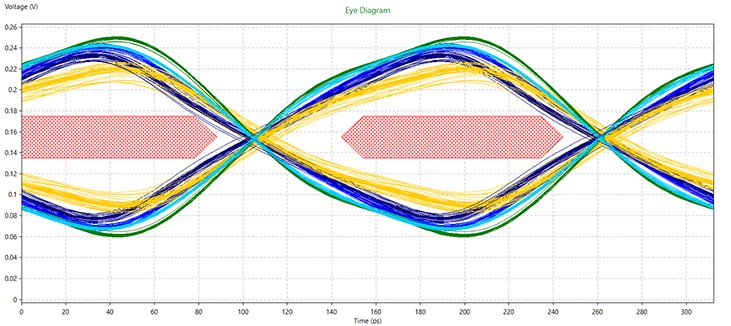
The designer can examine the bus responses from the circuit simulation and check the eye mask to ensure it fits (Figure 7).
After running the initial simulation, the next step is to run a circuit/channel correlation. This is also easily done in the workflow, with the tool doing all the setup and simulations automatically and providing a view of the overlay for comparison (Figure 8).
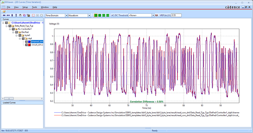
A match of 3% or better is needed to qualify the usage of the channel simulation and move to the next step, because, ultimately, a channel simulation of millions of bits will be run to see if the GDDR6 specification for the BER eye mask and eye opening is met. Selecting the different options for ramp response will allow the SI engineer to find the best option for achieving correlation within tolerance.
Next, a channel simulation is run, examining various AMI model configurations to determine the need to enable equalization settings. The tool can disable any of the AMI models and run a baseline simulation to determine if equalization is needed for the controller, memory, or both (Figure 9).
Once the equalization needs are determined, a what-if analysis can be run to change the AMI parameters, and examine its effect on the eye opening or sweep certain AMI parameters. Multiple parameters can be swept, including AMI parameters. In this example, a sweep was performed of the transmit and receive AMI parameters with three step counts each, which produced nine iterations. The results are overlaid, enabling the designer to determine the simulation that gave the best result and set those values in the AMI model.
After determining the proper AMI parameter, the designer runs a channel simulation to examineis the waveform and the eye opening (Figure 10).
The number of bits used for the eye diagram can be specified, with the default being the last 1,000 bits saved. Other results returned by the tool include the bathtub curve and a report of the eye height opening for the different signals to examine the reduction in eye height with higher BERs.
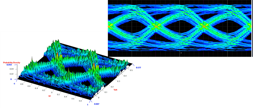
Figure 11 is an eye display showing the distribution of noise and jitter in both 2D and 3D views.
After running the channel simulation, the designer performs an additional characterization of the bus as part of the workflow to capture the crosstalk in the individual signals. Because this is a channel simulation, the crosstalk needs to be characterized a little differently than the circuit simulation, which is embedded.
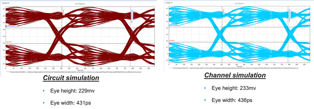
Figure 12 compares the circuit and channel eye measurement simulations, which correlate well with the eye height and width. This gives the designer confidence that million+ bit simulations can be run to capture the impact of crosstalk on the BER. This is essential to understanding how the design will run in the field and ensuring that the GDDR6 compliance requirements are met.
The next step in the workflow is to include power noise effects in the channel simulation. Until now, an ideal power (VED and VCC) for both the controller and memory design has been assumed. The power noise is affected and needs to be included in both the circuit and channel simulations. The channel simulation power effects are captured through characterization, whereas the circuit power effects are captured through the interconnect model itself. To verify the power noise in the channel, two channel simulations are run, one with ideal power supply and one with non-ideal power supply. The results enable the designer to compare the characterization responses and other channel simulation results to see the effects of non-ideal power on the eye opening (Figure 13)
Once this step is complete, a report can be generated for compliance check and signoff. The GDDR6 JEDEC specification is built into the report generation, and an enhanced data-rate-dependent measurement is included. The report highlights any violations. Any signal can be selected within the report table to view the eye opening with the mask automatically calculated. If there is a violation, what-if analysis can be performed to obtain a solution.
PI Testbench for GDDR6 Memory Interface
Many signal integrity designers are also responsible for power integrity. The GDDR6 testbench example can also be used to verify sufficient, efficient, stable, and reliable power delivery through the PCB and IC package for power integrity signoff (Figure 14).
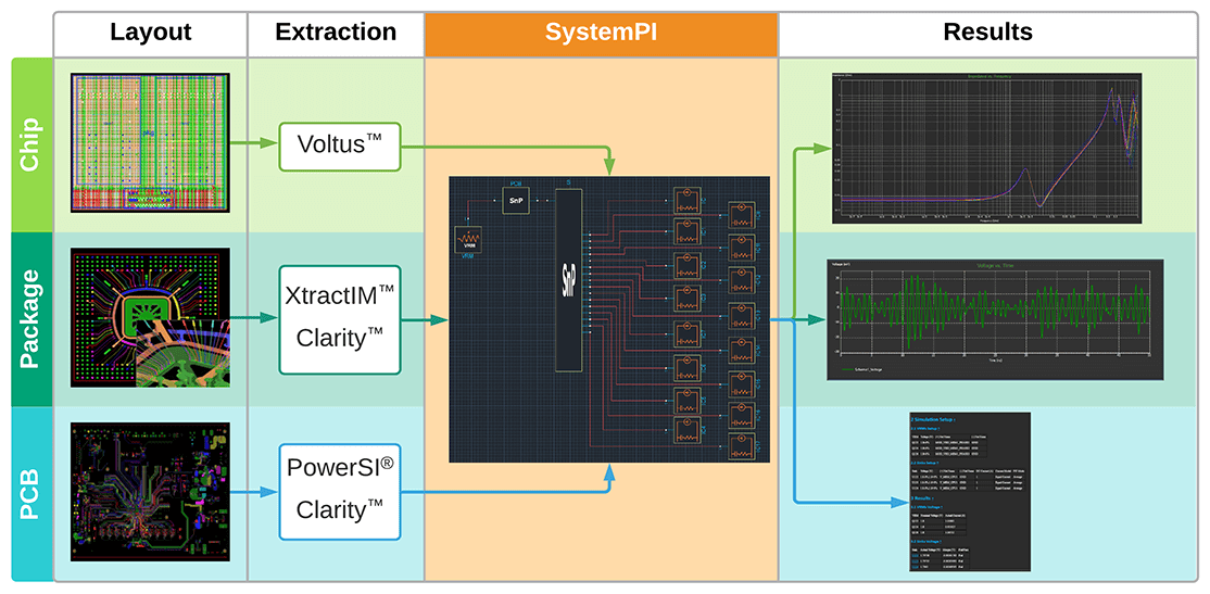
From a signal integrity perspective, simulation is performed from the transmitter to the receiver. For power integrity, simulation is done from the voltage source or voltage regulator module (VRM) to the voltage sink (component pins). The new topology-based user interface makes it easy to connect multiple fabrics across cables, connectors, and multiple fabrics such as PCB, package, interposer, etc.
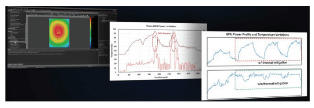
Proper power integrity analysis needs to be thermal aware. IR drop analysis should be integrated with thermal analysis. Cadence Celsius PowerDC and Celsius Thermal Solver provide electrothermal co-simulation as well as 3D thermal insight from a common user interface used by other Cadence analysis tools (Figure 15).
Conclusion
The memory interface roadmap is constantly advancing. The GDDR7 specification that will likely support 1.5TBps is under development, and Micron and NVIDIA are already producing the interim GDDR6X samples at 1TBps. The move towards pulse- amplitude modulation 4 (PAM4) used in GDDR6X and GDDR7 will encounter new challenges. Cadence is advancing parallel bus analysis technology by utilizing its many years of experience in PAM4 simulation for serial link analysis. As the worlds of serial link and parallel bus continue to blend, Cadence will be ready with tools used internally to support cutting-edge memory interface challenges.
The GDDR interface has evolved beyond the original applications that addressed the need for fast data access for data-hungry GPUs for gaming applications. Today, design software leverages GDDR6 for many high-performance applications, including automotive, HPC, AI/ML, and 5G. Design teams can confidently utilize a holistic solution from Cadence for memory interface design and analysis challenges, including IP, systems on chip (SoCs), interposers, IC packages, and PCBs.