With growing on-chip radio frequency (RF) content, electromagnetic (EM) simulation of the passives is critical for a variety of reasons – from selecting the right RF design candidates to detecting parasitic coupling that directly impacts performance. Being on-chip, accurate EM analysis requires a tie into the process technology in the form of process design kits (PDKs) as well as a foundry-certified EM simulation technology. Anything short of that could very well compromise the functionality of the RF integrated circuit (IC). More than 10X faster than other commercial EM tools, the Cadence® EMX® Planar 3D Solver is the fastest EM simulator for IC design based on fast multipole methods (FMMs) and provides the highest-in-class accuracy because of volume mesh formulation for conductors.
Introduction
With growing on-chip radio frequency (RF) content, electromagnetic (EM) simulation of the passives is critical for a variety of reasons – from selecting the right RF design candidates to detecting parasitic coupling that directly impacts performance. Being on-chip, accurate EM analysis requires a tie into the process technology in the form of process design kits (PDKs) as well as a foundry-certified EM simulation technology. Anything short of that could very well compromise the functionality of the RF integrated circuit (IC). More than 10X faster than other commercial EM tools, the Cadence® EMX® Planar 3D Solver is the fastest EM simulator for IC design based on fast multipole methods (FMMs) and provides the highest-in-class accuracy because of volume mesh formulation for conductors.
Obviously, the term RF covers radios of all types, but as old-timers say, “digital signal frequencies are in the range that we used to call microwave”. So, if you are designing a 112Gb/s SerDes then you are dealing with the same type of frequencies as 5G mmWave. In fact, serial interfaces are likely to get more like radios in the future, since the smart money is on next-generation interfaces using quadrature amplitude modulation (QAM) rather than PAM8, thus making use of phase as well as amplitude. QAM is used by all mobile phone radio interfaces.
RF design involves passive components, including resistors and capacitors, but also inductors, transformers, and BALUNs. A BALUN is a special type of transformer that converts between a BALanced and UNbalanced signal. Older processes, with thin metal and low-resistivity substrate are not really suited to creating these structures efficiently on chip.
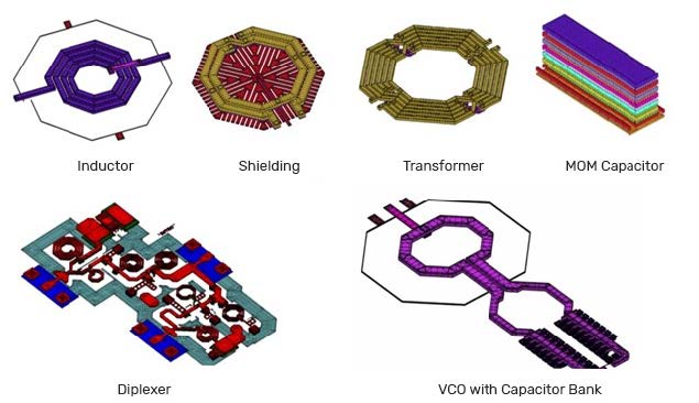
Once CMOS processes were fast enough that designers could even think about designing much of an RF circuit on-chip, these passive components remained on the board (or inside the package). But modern processes allow these components to be created on-chip with equivalent insertion loss to external components for many frequencies, as well as a lower cost due to saving not just the external components but the I/Os required to access them. In addition, modern processes with large numbers of metal layers allow high-density metal-on-metal (MoM) capacitors to be manufactured in the interconnect stack. Figure 1 shows the types of passives that can be analyzed, from more basic ones in the top row, to more complex ones in the bottom row.
EM Simulation
Obviously, fast and accurate modeling of these integrated passives is important. There are three main aspects to this:
All analyses follow roughly the same game plan. An EM solver first takes in a physical description of the conductors, typically layout, although for something like a connector it is actually a mechanical model. The EM solver calculates the S-parameters for the geometry by numerically solving Maxwell’s equations. S-parameters are the common method of describing the behavior of EM performance of RF components, in that they give the ratio of the reflected to incident power at the various ports. Maxwell’s equations are the underlying physical equations for electric and magnetic fields. Since the solution is numerical, the problem must be broken up into small volumes and/or surfaces, so that there is a finite number of unknowns. The most general way of accomplishing this, is to use a finite element method (FEM), which is the method used in the Cadence Clarity™ 3D Solver.
All of the space is meshed in 3D tetrahedra in these methods, including the dielectrics and air regions above. Of course, a boundary is used at the edge of the problem as one must truncate the size of the problem. However, if the geometry is planar, meaning the dielectrics of the metal lines are placed on layers that are flat and homogeneous, Maxwell’s equations use moment methods. These methods use the concept of a Green’s function to pre-compute the effect of the various dielectrics. The metal is meshed (as opposed to all of space), and the interaction between all currents on the cells is calculated. This results in a tremendous speedup of solution and a reduction of memory usage as compared to FEM methods. The designer is taking advantage of the planar geometry of the silicon chip.
The EMX Planar 3D Solver further speeds up the process by solving the matrix equation using FMMs. These methods speed up the solution of the problem by taking advantage of the unique properties of matrices resulting from Maxwell’s equations. Additionally, it takes advantage of any symmetries in the geometry, which results in not having to recalculate identical interactions between similar meshes.
The EMX Planar 3D Solver provides EM analysis of on-chip passive RF structures, which are increasingly moving on chip. Integral formulation (sometimes called boundary element) approaches like the EMX Planar 3D Solver are most appropriate when the enclosing dielectric is largely planar. Of course, ICs are certainly largely planar, and the passives are all planar. At the next level of detail, semiconductor layers really are (almost) planar, with vias between the planes. The EMX Planar 3D Solver uses an FMM algorithm computational software, which is both faster and more accurate than doing a fully general 3D analysis and can often take advantage of the planarity.
To perform the analysis of on-chip RF components, PDKs are required. The EMX Planar 3D Solver uses PDKs from almost all processes that are used for building such components. Of course, RF generally does not use the most advanced nodes since there is no advantage – an inductor is the same size whatever the process, for example. Also, advanced FinFET processes have lower voltages so are less effective for building power amplifiers, and the higher gate resistance makes them less effective for low-noise amplifiers.
While ICs are more than mostly planar, they have other advantages that can be used to optimize calculation:
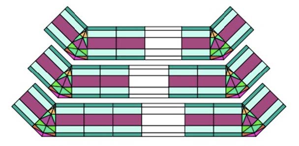
As an example of the regularity that the EMX Planar 3D Solver exploits, Figure 2 shows a wire mesh with the isomorphic shapes colored. The EMX Planar 3D Solver takes advantage of this regularity to avoid repeating computations, reducing both the runtime and the memory requirements.
However, not everything is well-behaved on an IC. The biggest issue is variability during manufacture, which deserves a section of its own. Attention also is needed in a few other difficult areas:
Variation
Advanced semiconductor processes are not completely perfect as there is variation from wafer to wafer and even die to die. The physical width, thickness, and resistance of a wire varies statistically, and can also be affected by the surrounding wiring. This is especially true below about 28nm where optical proximity correction (OPC) is required because the feature sizes are smaller than the 193nm light used for the lithography. It is even more true at 16nm and below where multiple patterning is required on some layers. (EUV probably improves this but RF experience with chips built using EUV, second-generation 7nm and below, is limited.) Some factors, such as sheet resistance, can vary significantly from their nominal value. Clearly, these large variations can affect the EM performance and so it is important to account for them in simulation and modeling.
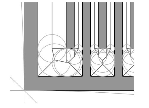
Foundries provide detailed information about pattern dependencies, usually in the form of tabulated data indexed by wire width and spacing. Internal to the EMX Planar 3D Solver, the input drawn layout is automatically modified using these tables to accurately model the structures that will actually be fabricated. For simple layouts, such as multiple parallel wires, terms like width and spacing have obvious meaning. But the EMX Planar 3D Solver must handle more complex layouts involving non-uniform structures, but using only tables indexed by width and spacing. To handle this, the EMX Planar 3D Solver uses Voronoi diagrams to analyze and partition the layout into non-overlapping regions. Then maximally sized circles can be inserted, and these can be taken as local approximations of the spacing. The local width is calculated in a similar way with circles inside the conductor. Figure 3 shows an example (showing only the spacing circles).
Typically, the most significant fabrication effect is that the manufactured line width varies from the drawn width by a bias amount that depends on the local width and spacing in the layout. The bias amounts come from the table already described above. The table, being tabular, only has certain values and interpolation is used to compute bias as a continuous function of (drawn) width and spacing.
An Example
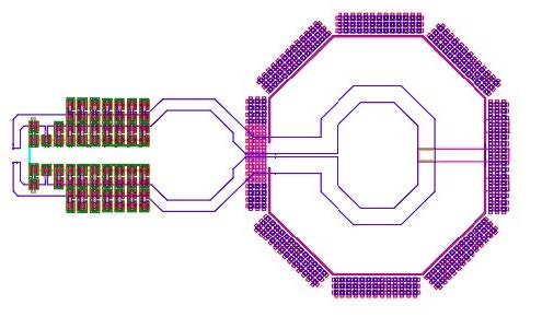
As an example, let’s use the voltage-controlled oscillator (VCO) that appeared right at the start of this post as an example of the sort of structure that the EMX Planar 3D Solver can analyze. Figure 4 shows the VCO fabricated in a 6-layer 90nm CMOS technology. It consists of an inductor and a bank of 66 MoM capacitors that are switchable for tuning. The inductor is small enough that parasitic coupling between the inductor and the interconnect and the details of how the capacitors are hooked up must be considered. Indeed, a block-by-block model failed to predict the VCO’s behavior.
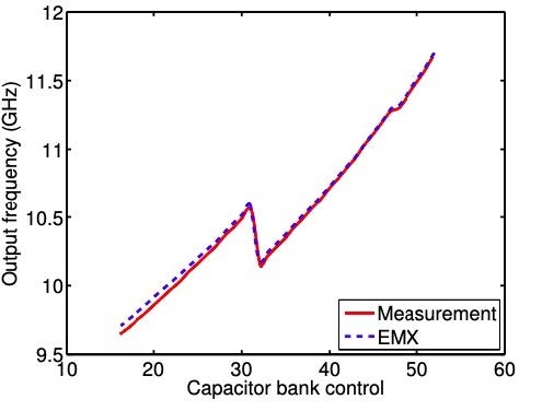
However, using the EMX Planar 3D Solver to simulate the whole structure at once gave accurate results. The simulated and measured tuning curves are shown in Figure 5, where the red line shows values measured from silicon; the blue line shows values calculated by the EMX Planar 3D Solver.
Integration
With the EMX Planar 3D Solver integrated into the Cadence Virtuoso® Custom IC Design Platform, you can work on layout of your design or a particular passive, and then perform analysis without leaving the Virtuoso environment. You can also use Cadence Spectre® simulation technology to create models of the results of the EMX Planar 3D Solver analysis and then simulate them (along with other Spectre models).
Conclusion
More than 10X faster than other commercial EM tools, the EMX Planar 3D Solver is the fastest EM simulator for IC design based on the FMM and provides the highest-in-class accuracy because of volume mesh formulation for conductors. The EMX Planar 3D Solver is supported by all foundries and extensively validated against silicon measurements, with PDKs available, and is seamlessly integrated in the Virtuoso environment for ease of use.
