White Paper
How to Achieve 10X Faster Power Integrity Analysis and Signoff
In our mobile computing era, system-on-chip (SoC) design has become much more complex, with challenges from complex design rules on advanced process nodes, low-power circuitry design techniques, and increasing circuit sizes. Power integrity is a crucial part of successful design signoff. This paper discusses a new tool that speeds power integrity analysis and signoff by 10X compared to other technology available, while still providing SPICE-like accuracy. The tool integrates with a full suite of design implementation and signoff tools, together overcoming signoff challenges to deliver the industry’s fastest design closure flow.
Overview
Introduction
System-on-chip (SoC) complexity has taken on a new dimension in the face of mobile computing requirements. As consumers come to expect smaller, higher performing devices with long battery life, the chips that fuel these products must also be more function rich, consume less power, and come in smaller form factors. For design engineers, these changes mean applying advanced power techniques (such as power-gating switches), increasing the intellectual property (IP) content and functionality (such as analog/mixed-signal macros), and dealing with tighter design margins (such as sub-1V power supplies). On the other hand, the time-to-market requirement continues to be aggressive, which makes the end-of-design cycle’s power signoff step as critical as ever for a successful tapeout.
The power signoff technology available to date has not kept pace with the speed of innovation. Extra runtime, for example, has always been a bottleneck that prevents designers from performing complete and thorough power integrity analysis and optimization. However, a new tool now available utilizes advanced massively parallel algorithms and a hierarchical architecture to provide up to 10X faster power integrity and analysis signoff with SPICE-like accuracy. Additionally, the tool is part of a complete chip-to-system flow that speeds up the design closure process by enhancing productivity throughout the cycle.
Growing Design Complexity Calls for New Power Integrity Analysis Tools
The combination of growing design complexity and size with more complex analysis requirements is causing an increase in the time it takes to perform power integrity analysis and signoff. A “flat” methodology, where the design is flattened down to one top-level layer, isn’t sufficient for analyzing extralarge designs with hundreds of millions of instances. Current solutions tend to be segmented “point tools” that do not deliver the accuracy or ease-of-use required to keep up with the demands of advanced SoCs.
What’s more, current solutions, because they are point tools, don’t provide an efficient means to assess the impact of power on timing closure. Yet, timing is most sensitive to the power supply (VDD). There are also new challenges resulting from advanced-node design technologies and techniques, such as the FinFET process and 3D-IC packaging. With FinFET devices, for example, there are new electromigration rules arising from vertical current directions, increased power density, etc. With 3D-IC, there is a new requirement for electrical-thermal co-simulation. To enable design engineers to meet time-to-market and quality demands, the need has emerged for a complete power integrity analysis solution, spanning chip to package to system.
What Makes an Ideal Power Integrity Tool?
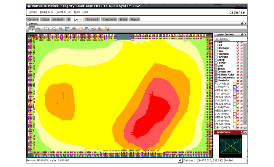
A design can fail when it encounters scenarios such as increased leakage, temperature variations, or decreases in operating voltage because of static and dynamic IR drop. Being able to debug and verify that power and IR drop constraints are met across multimillion-gate designs and multiple die—early in the process—is key to saving precious development costs and time. In other words, finding the “hot spots” on the chip early on can help prevent chip-performance degradation.
To properly support advanced SoC designs, the ideal power integrity analysis tool should be able to:
-
 Calculate leakage as well as switching and internal power consumption across the chip
 - Perform power integrity analysis (IR drop and electromigration checks) on the power grid
- Optimize the current flow of the design’s physical implementation by recommending ideal size and placement of decoupling capacitor cells and power-gating switches on the circuitry
- Assess the impact of IR drop on design closure including static timing analysis
Using production-proven, signoff-quality algorithms and engines, Cadence has developed a new full-chip, celllevel power integrity tool that provides all of these functions. The Voltus IC Power Integrity Solution delivers up to 10X faster power integrity analysis performance compared to competitive solutions. The tool provides SPICE-like accuracy and has been certified by TSMC for its 16nm FinFET process. As such, engineers can be confident that the tool will be accurate across different design rules.
Massively Parallel Execution Yields Faster Performance
Compared to other technologies available, Voltus IC Power Integrity Solution delivers advances in performance, accuracy, and closure. On the performance front, the tool uses advanced massively parallel algorithms to deliver 10X faster performance than competing solutions.
As an example of the faster performance, consider a very large design with several hundred million instances at an advanced process node from an early beta customer. With an existing production flow, hierarchical static and dynamic power signoff would take ~10 days to complete. Voltus IC Power Integrity Solution finished the task in just 26 hours on 32 CPUs—a ~10X speed up, resulting in a successful tapeout ahead of schedule.
Now, let’s take a look at a static power-analysis example, featuring an analog/mixed-signal chip with 27 million instances at the 40nm node. The existing production flow completed analysis in 58 hours. By comparison, Voltus IC Power Integrity Solution finished the task in less than 6 hours on 8 CPUs—a 10X speed up—with the same level of accuracy.
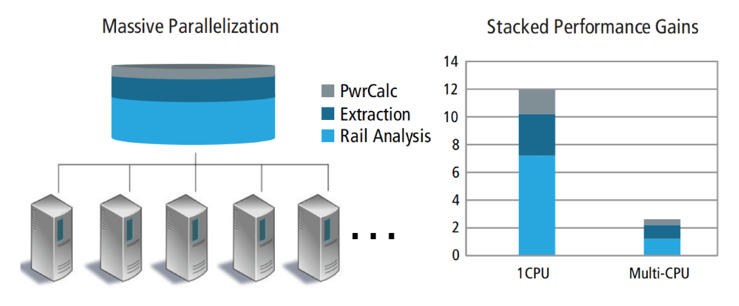
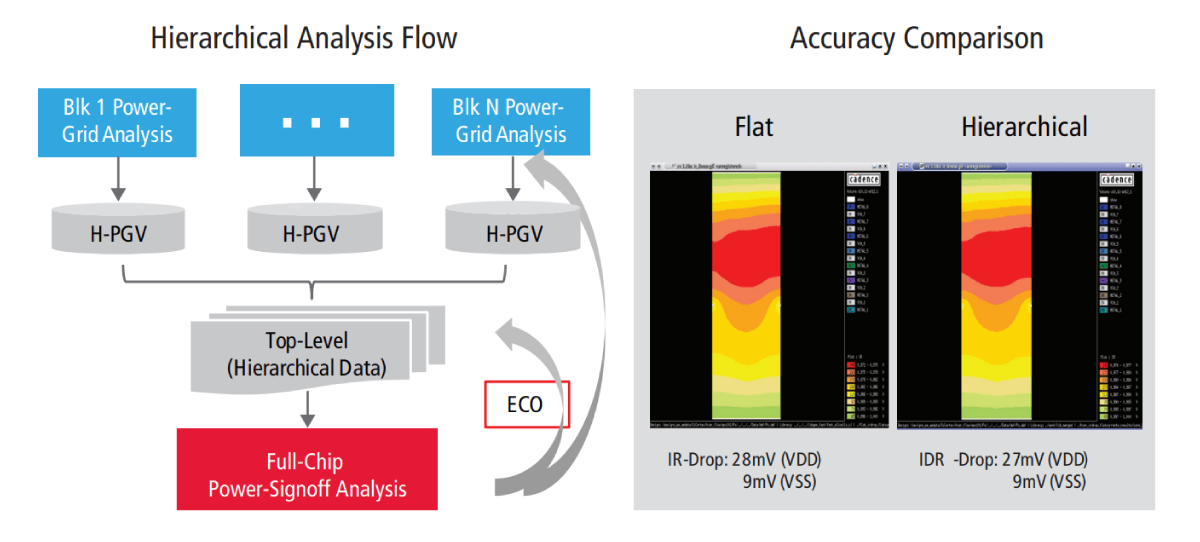
The performance level of the tool extends across a computer network and at high capacities—up to one billion instances—due to the tool’s hierarchical architecture. For example, if a single machine has as many as 16 CPUs, Voltus IC Power Integrity Solution can run on all of these CPUs simultaneously. If there are a few machines, each with multiple CPUs, linked in a network, the tool can still support fast power-analysis computation using its multithreaded, distributed-processing techniques. With the hierarchical approach, one can build a power-grid model, representing the lower-level part of the design hierarchy with power-grid information of interest. This model reduces the overall number of nodes viewed at the top level and, as such, enables the engineer to run much larger design instance numbers in the analysis than competitive solutions can accomplish.
In terms of closure, the Voltus tool offers early grid rail analysis in the floorplanning and power-planning stages, physically aware grid optimization through place-and-route engineering change orders (ECOs), and chip and system co-design analysis. As for its high accuracy levels, Voltus IC Power Integrity Solution features a SPICE-level rail matrix solver, along with accurate power-grid RC extraction and instance power calculation and distribution. Using sophisticated algorithms, the rail matrix solver can support dozens of CPUs distributed across multiple machines, providing highly accurate simulation of the power grid in large networks.
Part of a Complete Signoff Flow
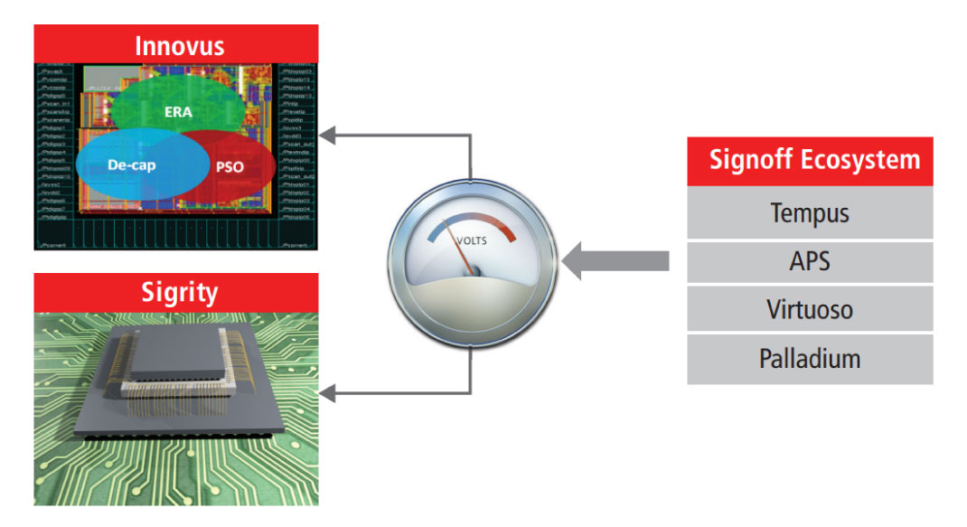
Voltus IC Power Integrity Solution is an integral part of a complete signoff and design closure flow offered by Cadence. The tool is beneficial as a standalone power signoff tool. However, its integration with other components provides design engineers a productive and fast design closure process, from chip to system.
Early rail analysis
In a traditional design flow, an engineer would complete the placement and routing step and then proceed with power signoff analysis to assess the viability of the power grid. But if a problem is found after power integrity analysis on a completely placed and routed design, it could take longer to resolve or even be irreparable. Because Voltus IC Power Integrity Solution is also integrated with Cadence Innovus Implementation System, design engineers have a unique capability that brings power-grid design to the early stage of physical implementation. Early rail analysis considers floorplanning information, as well as the size and location of the power-grid metals. If the engineer has to place two function blocks together (and both are very active), the integrated solution provides guidance on how best to apply placement and routing on the grid. A positive early rail analysis result can encourage power signoff to converge faster and, thus, speed-up design closure.
Real-world peak power analysis
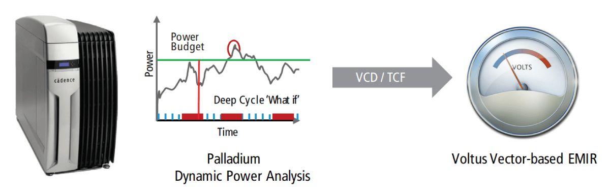
Power integrity issues such as IR drop and electromigration, if left unresolved, can cause silicon failure. Using realworld stimulus can improve accuracy of results, especially when considering chip behavior over a long period of time and observing where peak power consumption occurs due to increased activity.
The combination of Cadence Palladium emulation technology and the Voltus solution can deliver highly accurate IC power integrity analysis, driven by real-world power stimulus from the Palladium platform’s “deep cycle” Dynamic Power Analysis (DPA) capability.
Unified electrical signoff
Timing is most sensitive to the power supply. As such, a lack of accurate, effective power-supply values to instances along a power grid can lead to design guard banding, which increases pessimism in static timing. Since Voltus IC Power Integrity Solution is integrated with Cadence Tempus Timing Signoff Solution, design engineers gain a unified power and timing analysis and closure system. The integrated solution increases accuracy in static timing analysis by up to three percent, reduces timing pessimism, and yields a more realistic voltage drop across the chip.
Chip-package-PCB co-simulation and analysis
To prevent thermal crashes of packages and other power integrity issues at the chip and PCB stages, the tool is integrated with Cadence Allegro Sigrity technology to provide chip-package-PCB co-simulation and analysis. The integrated solution promotes accuracy in the power-grid networks for chip and board, and includes support for advanced packaging technologies such as 3D-IC. By using these tools together, engineers can achieve faster system-level power integrity analysis and closure.
Summary
More complex and time-consuming power integrity analysis calls for a more efficient analytical tool. The demands of mobile and Internet of Things applications are creating more pressure to deliver products to market faster and with higher performance. By utilizing advanced massively parallel algorithms, along with up to one billion instances in capacity and a hierarchical architecture, Voltus IC Power Integrity Solution delivers 10X faster power signoff than competing solutions. Integrated with other key timing analysis, physical implementation, simulation, and packaging tools to form a signoff ecosystem, the resulting solution provides the industry’s fastest design closure flow.
Further information
To learn more about achieving faster power analysis signoff, visit: Voltus IC Power Integrity Solution.