White Paper
Cloud—The Future of Electronic Design Automation
Design complexity and competitive pressures are driving electronics developers to seek innovative solutions to gain competitive advantage. A key area of investigation is applying the power of the cloud to electronic design automation (EDA) to dramatically boost productivity. While hosting production designs and EDA workflows in the cloud for over a decade, Cadence has internalized the unique challenges of EDA cloud users and the essential cloud capabilities necessary to successfully resolve them. This whitepaper summarizes these unique EDA requirements and solutions to help you in your design team’s cloud journey.
Overview
Bridging the Compute Gap
Driven by a series of innovations during the past decade, the size, complexity, and variety of integrated circuit (IC) design continues to increase exponentially. Meanwhile, intense competitive pressures force companies to make the most of every dollar of capital and every talented engineer on their staff. In response to these forces, some companies have simply been eclipsed or absorbed by competitors, while others have attempted to tackle these core issues. One such area that electronics developers are rethinking is the compute infrastructure model of company-owned, housed, and run datacenters.
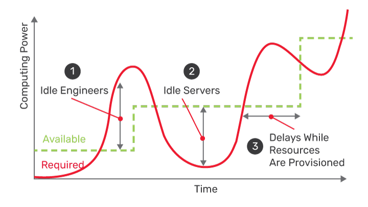
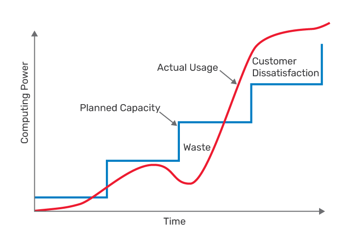
IT and CAD teams struggle to meet the peak EDA compute needs of their engineering teams when limited by the finite space and capacity of on-premise datacenters, regardless of company size or resources. Yet, despite this widening compute gap, engineering teams must still meet their demanding product design deadlines and time-to-market expectations regardless of an aging or limited infrastructure that can severely hinder their productivity.
An attempted solution to limited engineering productivity is to refocus more engineers or tools to the highest priority project, but this makes the compute gap worse. More engineers running more tools on the same scale of infrastructure only leads to more compute resource contention, poorer performance, and, ultimately, less engineering productivity. Even when the infrastructure is identified as the issue, few companies have the resources to refresh and grow their hardware environment fast enough to meet the ever-increasing peak demand for compute resources. Even for the few companies who do have the resources, access to the new hardware for peak need is not instantaneous; it must be quoted, ordered, received, installed, and configured—which can take months—before it can begin to ease the productivity bottleneck.
The ultimate solution to bridging the compute gap—perhaps the only solution—is to move EDA to the cloud. Indeed, we at Cadence believe that the future of EDA will unfold in the cloud.
Unique Requirements
Since starting in the early 1970s, EDA tools and flows have been synonymous with distinct and demanding compute needs. Early computer-aided design (CAD) activities were largely done in massive corporate datacenters with proprietary tools. Even while these initial chips were mostly “hand-crafted” and limited to functionality that the human mind could comprehend, board-level and IC chip tools were still being created in-house. The early 1980s saw nascent EDA companies developing specialized workstations and interactive schematics, and layout design tools becoming more standardized. By the end of the 1980s, and with increased focus on IC designs, higher end workstations were being used to perform smaller scale simulation and analysis at an engineer’s desk, while larger analysis was still being done on corporate mainframe computers.
With chips crossing the 1 million transistors line in 1989 (with Intel’s N10 design), the EDA industry exploded in the 1990s. EDA offerings moved from point tools to flows, interplay between interactive and automated workloads increased, and chips regularly surpassed the hundreds of millions of transistors mark. These innovations led to new challenges and compute bottlenecks that in turn sparked more innovation—design hierarchies and cell libraries to address tool limitations, adding memory to improve productivity. By the 21st century, EDA had evolved further to support the development of the multi-core servers needed to run the growing internet and functionality like database searches. Systems on chip (SoCs) and a focus on system-level concepts were incorporated into EDA solutions, which in turn helped grow larger chip designs past the 1 billion transistor line (Intel’s Itanium).
By the early 2010s, new chip designs had grown to such an extent that the compute required to complete them in an acceptable amount of time had exceeded the average capacity of most design companies. This, paired with the innovations driven by the internet in the previous decade (higher bandwidth, consolidated regional datacenters) and the rise of cloud computing, seemed to suggest that EDA work would move easily and quickly to the cloud. However, until now, this has not been the case.
Concerns over the security of the cloud, of moving unique and business critical proprietary IP to a public cloud, have stalled this transition. While cloud computing seemed a logical choice for EDA work, this IP was not offloaded, and, ironically, business applications housing massive amounts of personal and business data moved to the cloud instead. As more and more personal data (from banking to health information, family photos to DNA records) have been moved to the cloud, largely through Software-as-a-Service (SaaS) business applications, perceptions of cloud security have shifted within the public generally and electronic design industry specifically. These more positive perceptions of cloud security, and the continuing internal compute capacity limitations, have set the stage for moving EDA work to cloud computing environments.
While simple in concept, moving EDA design and verification flows to the cloud is complicated by the unique requirements of the electronic design process. The sheer amount of data is one obstacle. Chip design “databases” are typically composed of large numbers of huge files, usually over-watched by sophisticated version management tools and distributed across worldwide design centers. Successfully building an efficient file system in the cloud to support EDA workloads requires considerable experience.
Another factor is the server, storage, and network expectations of the tools themselves. Each EDA tool has a unique set of hardware configuration needs to run optimally. To move to the public cloud, tool setup requirements must then be mapped to the chosen Infrastructure-as -a-Service (IaaS) vendor’s customized offerings—options that can vary across vendor. All these configurations require expertise when deployed in a commercial cloud environment, and unoptimized setups can lead to limited productivity gains.
Additionally, the inherent scalability of many EDA tools is limited by the developer’s assumptions about the reasonable number of servers that could be brought to bear on a problem. Tools are developed to meet the needs of real customers with real constraints. A few years ago, it would be viewed as a completely unreasonable expectation that a thousand servers could be brought to bear on a chip signoff closure task. Even the largest companies, whose internal server farms number in the thousands, must service many compute tasks across many projects and so cannot afford to devote a farm to discrete tasks. This thinking leads to tool architectures that limit scalability—thinking that must be changed.
Essential Capabilities
We at Cadence have experience supporting both our hosted customers and in-house engineers; this has given us the expertise to tackle the issues associated with moving EDA work to the public cloud. Having hosted design environments for over 100 customers during the last 10 years with our HDS business, we have seen firsthand the daily challenges our customers face: resource contention, limited capacity, and poor performance. As Cadence has grown rapidly over the past few years, the same pressures our customers experienced have also driven our internal R&D teams to make increasing use of the cloud, and to optimize our product architectures to support it. Since 2014, Cadence has supported public and private cloud environments for our own engineering teams—both developing our tools and running them within a public cloud environment.
This experience has led to the firm conclusion that a successful cloud-based EDA solution must have four essential capabilities to successfully bridge the compute gap:
-
 Productivity
 - Scalability
- Security
- Flexibility
Productivity
For every company and project, managing time to market is critical. If a delay is caused by mismanagement, or even lack, of compute resources, market opportunities can be missed, and infrastructure investment can become worthless.
Also, for every dollar spent on commercial design technology, a greater amount is required to integrate and apply that technology to customer designs and environments. The organization must spend time and capital to acquire, integrate, deploy, and maintain these platforms for their engineering teams. They must hire and retain staff to support these environments and their engineering teams. And even with this investment, it is unlikely with the exponential growth of compute requirements for EDA work that in-house datacenters can support the peak needs of modern EDA workloads.
Inherently, the cloud provides the opportunity to focus scare resources on profitable design instead of expensive infrastructure. Rather than buy the infrastructure needed for peak, simply rent it. But achieving real productivity in the cloud for EDA users still requires experience and optimization. Experience is required to understand the differences in environment management on-premise versus in the cloud, and for understanding the various services offered by cloud providers. Cadence Cloud ensures this productivity boost and faster time to market by maximizing the benefits of cloud and enabling engineers.
Scalability
Electronic design covers a wide range of disciplines with customized tools and special requirements. Digital circuit designers use different tools and workflows than analog designers. Chip, package, and board designers all have different requirements. Those tasked with design verification in all its variations have yet other requirements. However, all these disciples must also come together at key intersections to enable the overall system design with milestone products being the SoC, PCB, and, ultimately, the hardware/software system that is the end product. So, one aspect of a viable cloud solution is that it be scalable in breadth to cover all these aspects of Intelligent System Design.
According to Daniel Nenni of SemiWiki, “…over the last ten years, we would ask customers how many simulations they ran, and the answer was always not as many as they would like due to time constraints. What that really meant is that they did not have enough software licenses and/or compute resources.”1 In addition, Richard Paw of DellEMC is quoted by Brian Bailey, saying that “…with EDA and chip design, you never are really done with verification. You verify to what you can afford. You have a set amount of money and you buy licenses and verify till you run out of money. You never get to the point of being happy, only good enough.”2 The question is whether “good enough” is sufficient.
Another aspect of scalability is accommodating the brute force compute capability of the cloud. Whereas most engineers are limited to running their tools on perhaps tens or, in rare cases, hundreds of servers, cloud-scale capacity is measured in thousands and tens of thousands of servers. Cadence Cloud makes the best use of the cloud infrastructure by selecting the right type and configuration of compute for the job—and scaling up or down intelligently based on the EDA tool and workload.
Security
Since the introduction of cloud computing, fear of compromising the intellectual property that was developed over years and at a high cost has slowed cloud adoption among semiconductor companies. However, the unspoken reality of the world today is that many companies struggle to keep up with the increasing number of security threats. They simply do not have the resources and expertise to keep in step with the constantly changing best practices. On the other hand, the largest and most profitable technology companies, the ones leading the cloud industry, have piled their resources into delivering the most advanced security measures available. The investments range from datacenter physical security rivaling military installations to sophisticated cyber security teams constantly on the lookout for attacks.
When the cloud was in its infancy, companies were hesitant to make the leap, mostly due to concerns about security. But now that the public cloud has matured—most companies already use the public cloud to store their financials, their patents, and their IP—engineers are coming to realize that using EDA tools in the cloud just make sense.
“People already put all of their most sensitive business data into the cloud, so this business model is becoming more acceptable,” says Frank Schirrmeister, Cadence’s senior group director for product management and marketing for emulation, FPGA-based prototyping, and hardware/software enablement. “Now we are seeing more openness to put designs in the cloud. Flexibility of access to faster execution is beating security concerns.”3
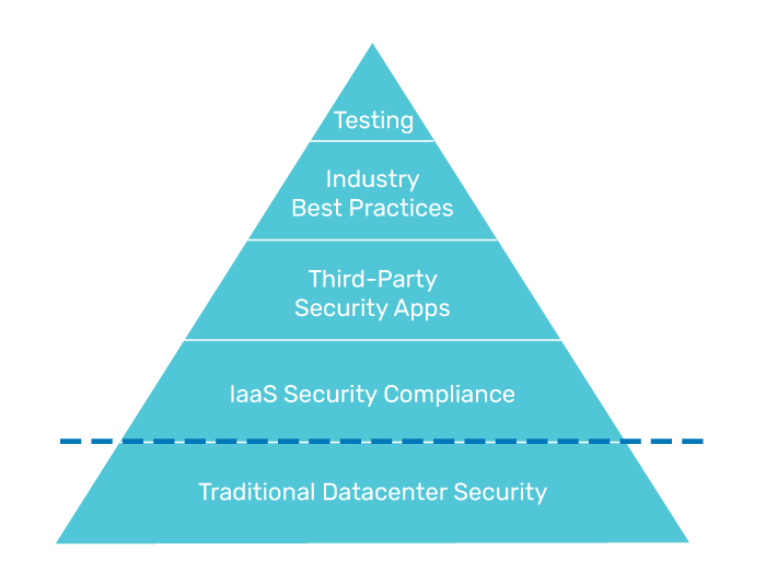
Cadence Cloud builds upon the native security of IaaS vendors, resulting from their investment in cloud security, through additional applications, best practices, and penetration testing.
Flexibility
Since electronics design is undertaken by startups as well as multinational corporations, some designing tiny IoT devices, while others developing the most advanced servers, a successful EDA solution for the cloud must be extremely flexible. Some companies will want to outsource all aspects of managing a cloud environment to get the largest productivity benefit, while others, who have already developed some experience in the cloud, will want to manage their own environments. Some organizations will want to move entire projects to the cloud, while others will only use it to address peak needs. Since there are excellent choices available for cloud service providers, customers need EDA solutions that are flexible enough to adapt to their requirements. Because of this, Cadence Cloud offers a variety of models—fully managed, self-managed, and mixed—at the tool, flow, and complete design environment level to support companies of any size, with any cloud vendor preference.
Cadence Cloud
We at Cadence have taken a leadership position in addressing the EDA challenges and bringing the benefits of the cloud to our customers with Cadence Cloud. This offering is the culmination of years of effort and we believe it represents the future of EDA. With Cadence Cloud, customers can finally bridge the compute gap and gain a dramatic increase in productivity. Early adopters of Cadence Cloud have reported unsurpassed productivity reducing peak need workloads, such as library characterization, from months and weeks to days and hours, and getting access to more compute in as little as five minutes.
The solution delivers intelligent scalability, with production-proven infrastructure software and services that provide optimum hardware resources and cleanly support mixed on-premise and cloud environments. With Cadence Cloud, customers can run the verification and simulations that are required by complex IC designs, scaling to fit the peak needs of this complex procedure, allowing designs to be tested and verified until “good enough” becomes “great”.
Cloud-ready tools with the latest scalable architectures, such as the Cadence Liberate Characterization Solution (library characterization), Xcelium Parallel Logic Simulation (digital simulation), Tempus Timing Signoff Solution, Quantus Extraction Solution, and Pegasus Verification System (physical verification) are just a few examples that enable scaling to hundreds and thousands of servers. Unique offerings such as Palladium Cloud and OrCAD Entrepreneur extend the power of hardware acceleration and online design capture to users hampered by traditional licensing approaches.
We’ve learned that requirements vary widely, and one size does not fit all, so Cadence Cloud provides flexibility to meet your needs. Whether you want a Cadence-managed solution or prefer a self-managed approach, want to move entire projects to the cloud or only offload specific peak demands, Cadence Cloud enables flexible licensing alternatives to provide a custom-fit solution.
Conclusion
The electronics industry has struggled to keep pace with rising IC complexity and intense competitive pressure. Companies seeking to excel in this environment are rethinking past assumptions with the goal of boosting their productivity and shortening their development schedules. Perhaps the most promising opportunity for these companies is to move their EDA environments to the cloud. Recognizing this opportunity and building on years of experience in providing hosted design environments to customers with HDS, we have introduced Cadence Cloud, a production-ready solution that delivers unsurpassed productivity, intelligent scalability, security you can trust, and flexibility to meet your needs.
In short, we believe that Cadence Cloud is the future of electronic design automation.
References
- D. Nenni, “EDA CEO Outlook 2018 Partly Cloudy,” Semiwiki.com, 16 April 2018. [Online]. [Accessed 16 May 2018].
- B. Bailey, “EDA in the Cloud, Part 2,” Semiconductor Engineering, 2 May 2018. [Online]. [Accessed 16 May 2018].
- E. Sperling, “Verification in the Cloud,” Semiconductor Engineering, 29 June 2017. [Online]. [Accessed 16 May 2018].
- B. Bailey, “EDA in the Cloud,” Semiconductor Engineering, 26 April 2018. [Online]. [Accessed 16 May 2018].
- Naresh Sehgal, John M. Acken & Sohum Sohoni (2015): Is the EDA Industry Ready for Cloud Computing?, IETE Technical Review, DOI: 10.1080/02564602.2015.1099056