White Paper
Best Full-Flow PPA
In the past few years, Cadence revolutionized the way digital designers could solve their design challenges by revamping the entire digital tool suite with key enhancements such as integrated engines, massively parallel processing, and early signoff optimization, all delivering faster turnaround time and best-in-class power, performance, and area (PPA) optimization. In the era of FinFETs and advanced nodes, these innovations enabled our customers to meet their stringent technical requirements and design chips that meet aggressive PPA goals. These have proved beneficial to customers as they design current and next-generation products. However, as we all know, the electronics-based world never sleeps and the push into bigger and more complex designs is unrelenting.
Overview
Industry Challenges
With the advent of new intelligent technology in the fields of high-performance computing (HPC), artificial intelligence (AI), automotive, and 5G, there is ever-growing design complexity that comes with its own set of technology and schedule challenges. New application-based architectures push the limits of current design tools and the requirements for PPA targets are much more aggressive than before.
Advanced-node processes provide designers the opportunity to improve performance, reduce power, and meet area requirements through new device and manufacturing innovations. However, nothing comes for free and the traditional design challenges at these smaller geometries don’t just increase—in some cases, entirely new process challenges are identified and need to be addressed.
Exploring Possible Solutions
As new architectures get developed, forward-looking estimation and predictability of downstream physical effects during the design exploration phase has long been a major challenge for system-on-chip (SoC) design teams. System-level verification tools can exercise real use cases, but they are disconnected from the implementation and signoff tools. Identifying and leveraging strengths of existing computational flow algorithms and bringing them upstream through a unification flow is one strategy that would mitigate some of the complexities seen downstream.
Unified Physical Optimization – “Start the Engines”
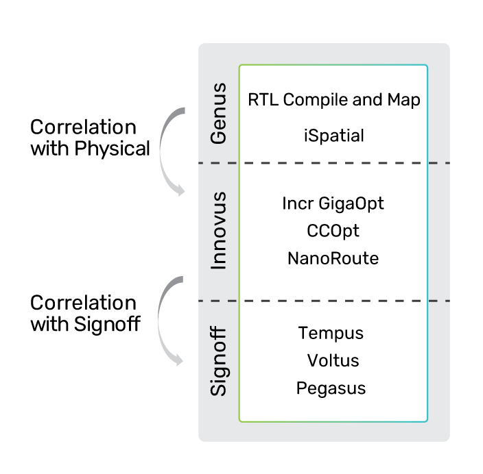
To address the ongoing challenges in the SoC design area, Cadence is leveraging computational software excellence to build on the integrated full-flow digital solution suite with new, smart innovations. The Cadence Digital flow has a strong collection of best-in-class computational engines embedded inside each tool, which work on separate objectives. These engines include the Cadence Genus Synthesis Solution’s structuring and mapping engine, GigaPlace placement engine, GigaOpt Optimizer, and NanoRoute Advanced Digital Router, each of which has innovative technology that was developed to solve optimization problems to meet PPA targets at a certain stage of the flow. To push PPA boundaries beyond set targets, there is need for these world-class engines to expand beyond the local workspace to different stages of the flow, in order to create a unified solution.
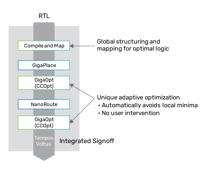
The “global mapping and structuring” engine in the Genus Synthesis Solution has advanced netlist structuring and optimization capabilities, as proven with deployments on multiple structured CPU designs. The numerical placement engine inside the Cadence Innovus Implementation System is the GigaPlace Engine, which takes into account multiple objectives like slack, wirelength, pin-access, and power, and excels in coming up with optimal placement aligned with routing requirements, thereby making the designs converge faster. The GigaOpt Engine used inside the Innovus Implementation System has unique adaptive optimization capabilities that automatically avoid local minima without any user intervention to get the best-in-class PPA results.
By merging these engine technologies, Cadence created the new iSpatial flow, which has a redesigned unified physical optimization technology across the Genus Synthesis and Innovus Implementation solutions, creating a seamless unified physical optimization flow from RTL synthesis to implementation.
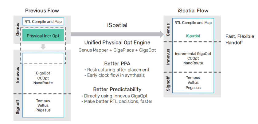
In addition, iSpatial technology has advanced “physical restructuring” capabilities which allow powerful large-scale logic restructuring to be done through all stages of the physical optimization flow, past clock tree insertion. The result is a redesigned and unified physical optimization flow where the first part of placement optimization is done in the Genus Synthesis Solution, with a flexible physical handoff to the Innovus Implementation System for incremental optimization to take the design to closure. Unified physical optimization also enables designers to leverage useful skew optimization in physical synthesis for another PPA boost.
This flow works with any design type—CPU, GPU, SoC, networking, AI cores, etc. The flexible handoff delivers the best turnaround time (TAT) and PPA for all work-group structures such as ASIC netlist handoff or complete front-end to back-end data sharing and flow development, as demonstrated by examples in the tables below.
| Signoff | Competing Technology | Cadence Digital Full Flow | Δ% |
|---|---|---|---|
| Fmax to goal | 89.4% | 98.1% | +10% |
| Total TAT | 300 hrs | 240 Hrs | -20% |
| Scripted | No | Yes | Repeatable |
| Signoff | Competing Technology | Cadence Digital Full Flow | Δ% |
|---|---|---|---|
| Fmax to goal | 94.7% | 97.8% | +3% |
| Total TAT | 81 hrs | 44 Hrs | -46% |
| Leakage | 41.62 | 40.71 | -4% |
| Scripted | No | Yes | Repeatable |
| Signoff | Competing Technology | Cadence Digital Full Flow | Δ% |
|---|---|---|---|
| Fmax to goal | 100% | 100% | |
| Total TAT | 100% | 65% | -35% |
| Total Power | 100% | 94% | -6% |
Machine Learning-Based Implementation
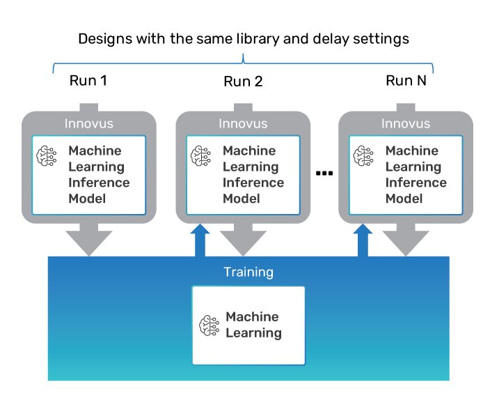
In addition to the unified physical optimization, the solution leverages deep learning algorithmic innovations to help customers address complex problems and exceed PPA within critical design blocks.
The integrated full-flow digital solution uses machine learning technology for accurate delay prediction and modeling that can help accurately model the pre- to post-route co-relation delays on critical nets, which help avoid surprises at later stages in the design. You can use the deep learning-based training infrastructure to “train” your design flow to capture relevant information and infer it during the actual implementation, thus helping reduce design margins and achieving better PPA.
For the first time, you have the benefit of customizing your implementation flow to improve current and future designs in order to get the best optimized PPA for your design type.
| Design | Node | WNS | TNS | Power |
|---|---|---|---|---|
| A | 8nm | 23% | 67% | 3.6% |
| B | 7nm | 5% | 77% | 3.4% |
| 5nm | 25% | 49% | 1.1% | |
| C | 12nm | 38% | 22% | 1% |
| Design | Node | Power | Area |
|---|---|---|---|
| GPU | 5nm | 8.5% | 8.3% |
| DSP | 7nm | 3.5% | 2.9% |
| ML | 5nm | 3.8% | 2.7% |
| Networking | 7nm |
5.1% | 4.4% |
New Logic Optimization
Customers making next-generation IP such as GPUs, DSPs, AI, and networking designs are using advanced features of System Verilog to streamline their RTL into as few lines as possible. RTL code with deeply embedded loops, operations on entire arrays, and many other complex functions are commonly seen with these new designs. If traditional methods for elaboration and mapping are used, they result in a large number of extra combinational logic stages, which may not result in an optimal architecture selection.
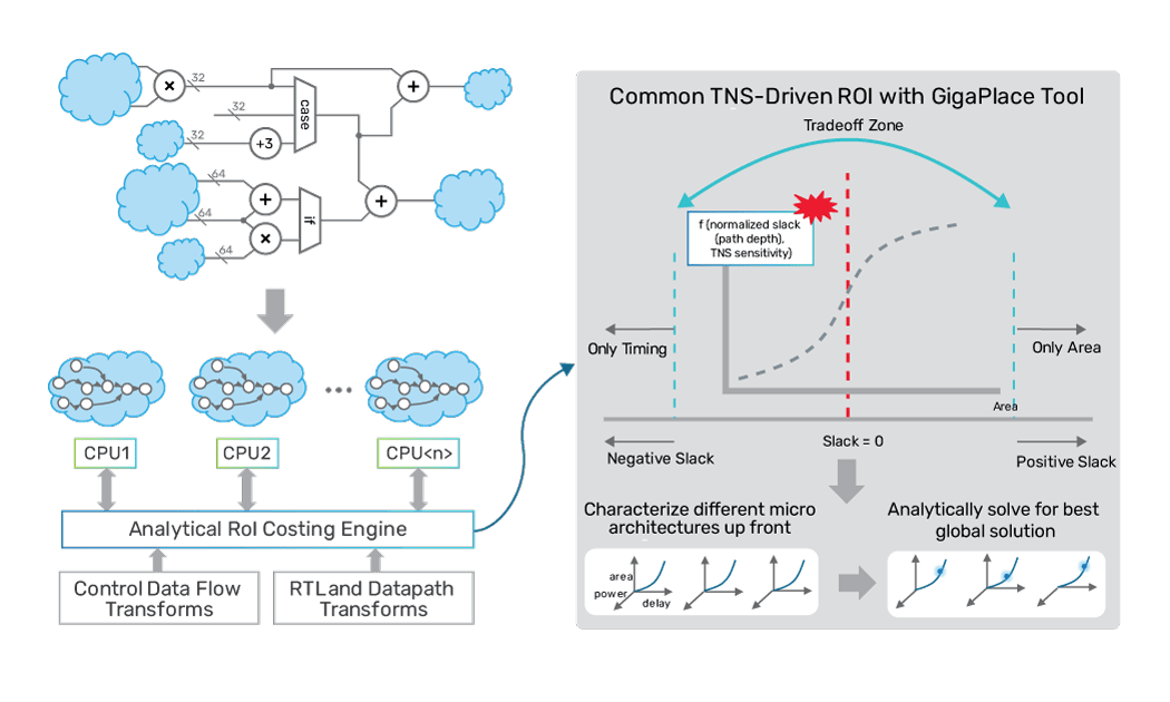
A new logic optimization engine inside the Genus Synthesis Solution provides an additional PPA advantage in the latest release. Compus advanced structuring optimization takes complex code and investigates multiple structures to deliver the best PPA for a given constraint set. It uses a unique TNS-driven ROI costing engine that is well aligned with the TNS-costing in the industry-leading placer inside the Innovus Implementation System’s GigaPlace Engine. The result is a netlist fabric that is more robust for optimization, delivering better power and area for some of the most area and power-sensitive designs.
Superior Signoff Convergence
As node geometries shrink with each next-generation design, a whole new list of electrical and timing checks comes into play. Particularly at 7nm and below, design engineers need to understand the high resistivity of interconnect layers and low voltage operation of the next-generation FinFET devices. These new design challenges make it impossible to separate timing and IR drop signoff. With increasing resistivity differences in the lower metal SADP or EUV layers, there is a significant impact that IR drop adds to design timing. Design engineers delivering the highest frequency silicon at advanced nodes are seeing setup-time failures in silicon, despite meeting traditional IR drop and STA signoff requirements. This max frequency failure is triggered by IR drop events, which cause a delay push-out on voltage-sensitive paths, but these failures are not typically found using current tools.
The traditional method of identifying critical timing paths or validating IR drop failures not exceeding 10% or so of supply voltage, and then separately validating setup time with a supply voltage date equivalent to the IR drop margin, falls short of identifying the complete set of paths. Also, closing them with a limited number of ECOs while opening a place-and-route design database is extremely time-consuming.
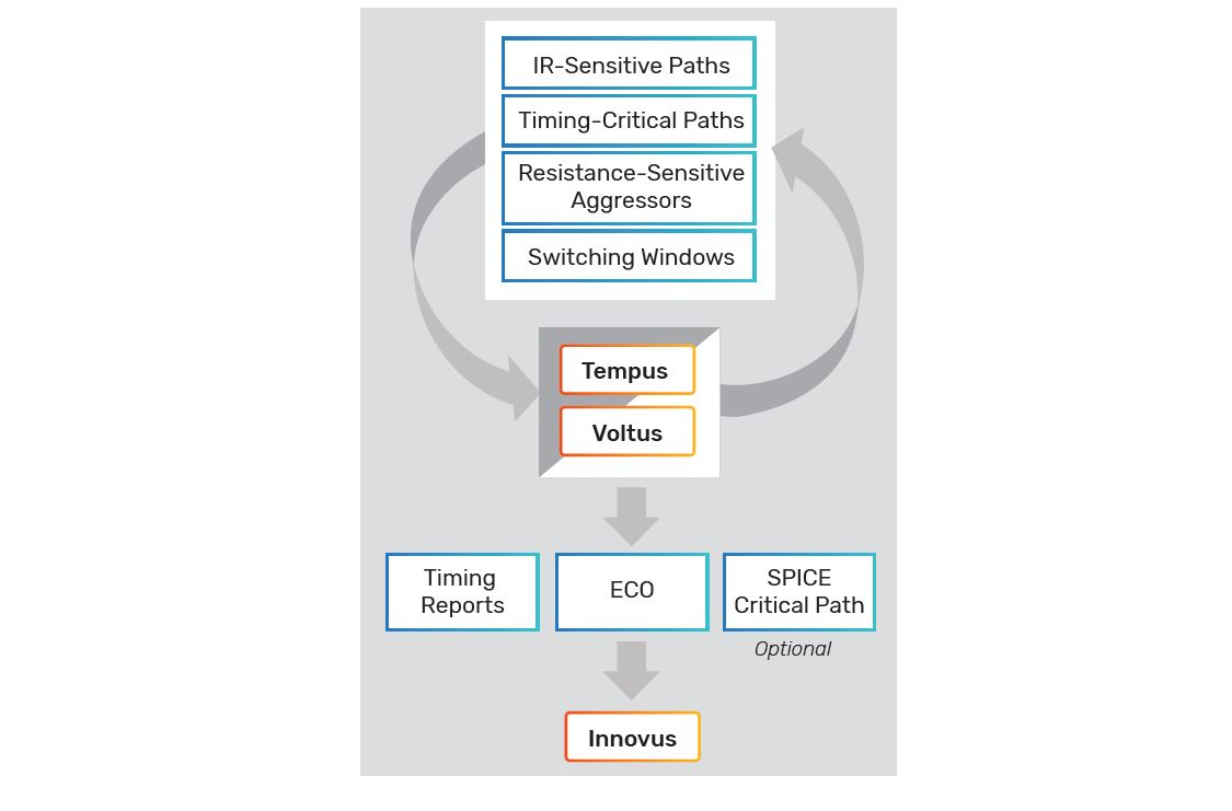
The integrated full-flow digital solution, with shared common timing and power engines communicating with each other seamlessly, provides a solution to these new design challenges. The Cadence Tempus Power Integrity Solution leverages the industry’s only tight integration between a signoff IR drop analysis tool (Voltus IC Power Integrity Solution) and an STA signoff tool (Tempus Timing Signoff Solution) to identify maximum frequency fails before tapeout. This tight integration also enables iterations between the two domains to identify IR-sensitive and timing-critical paths by identifying resistance-sensitive aggressors and aligning switching windows. The Tempus Power Integrity Solution offers a true signoff solution by natively finding possible escapes using a worst-case vectorless algorithm and then fixes these in the Innovus Implementation System with the Tempus Timing Signoff Solution’s ECO flow. This enables designers to find IR-delay push-out paths and catch potential silicon fmax failures before tapeout.
This unique design convergence flow, which starts working on a database already optimized by the iSpatial, machine learning, and Compus innovations, delivers the next-generation full digital RTL-to-GDS flow that can exceed stringent PPA targets.
Conclusion
Due to the rapidly increasing demand from growth markets like HPC, AI, and 5G, there is an increased demand for higher performance and higher quality designs with the lowest area and power footprints. Add to that the next generation of FinFETs and shrinking geometries, and customers’ design challenges can grow exponentially. These challenges need a solution that delivers something beyond traditional design automation.
Cadence’s integrated full-flow digital solution with unified physical optimization, logic structuring and deep learning technology embedded in the implementation flow can help push PPA beyond set targets. The solution delivers a 10 – 20% better PPA with the best turnaround time. With this new solution, customers can develop their next-generation design architecture with high confidence while achieving the set PPA targets. Customers can also rest assured that the natively integrated true signoff technology provides superior signoff convergence to close challenging designs with confidence while avoiding costly silicon re-spins.