White Paper
Automating Inter-Layer In-Design Checks in Rigid-Flex PCBs
Flexible PCBs (flex/rigid-flex) make it possible to create a variety of products that require small form factors and light weight, such as wearable, mobile, military, and medical devices. As flexible PCB fabrication technology has matured in response to demands for smaller, lighter products, new design challenges have emerged. This paper discusses some of the key challenges to address and also introduces a new PCB design approach that enhances productivity through in-design inter-layer checks required to ensure correct-by-construction design.
Overview
Introduction
Inside a variety of small electronic devices—from earphones to smartphones, tablets, and laptops—are rigid-flex PCBs comprised of rigid and flexible substrates laminated together. Such circuits are considered reliable, versatile, and space efficient. As designs continue to shrink for a variety of applications, this type of flexible substrate for electronic circuitry keeps growing in popularity, particularly in consumer electronics (Figure 1). Because of the bending possible with rigid-flex circuits, designers can place much more circuitry into the space available, even stacking the board layers in a 3D format on the rigid side. Multiple stack-up zones contribute to lower cost.
Traditionally, designers would integrate the flexible portion of their circuitry as a connector from one rigid board to another. However, flexible technology has matured substantially in recent years. Now, because of more stringent area requirements, designers are placing components on the flexible circuit area, using this area like a rigid substrate. PCB design technology to address rigidflex design has been available for some time. However, utilizing both the rigid and the flexible areas for components introduces new fabrication challenges that require more sophisticated PCB design technology.

Accommodating New Materials and Design Rules
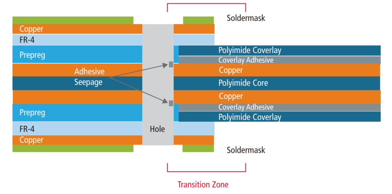
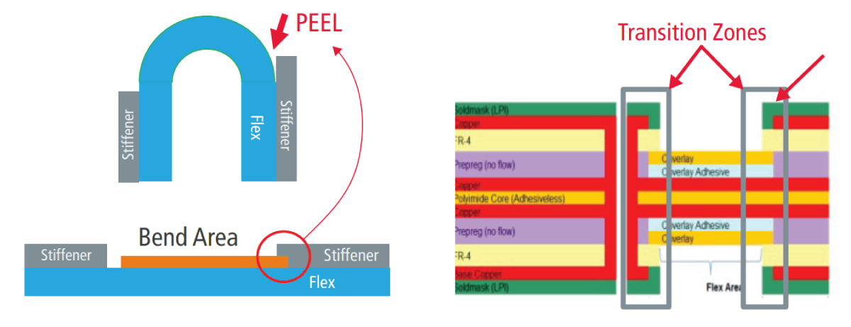
Rigid-flex PCBs consist of areas (zones) that differ in layer count and materials. Stiffeners bring rigidity to these PCBs, and are placed near or on the opposite side of components or near connector areas. They usually consist of a metal, such as stainless steel or aluminum, with the addition of dielectric material like a polymide build-up. The flexible portion of the design typically consists of a dielectric material with bend areas. The bend area must restrict the placement of components and vias; otherwise, these elements contribute to stress and cracking. Routing must cross perpendicular to the bend line to minimize material stress at this location. Adjacent layer routing through the bend area should be offset to prevent what is called the I-BEAM effect. Traces routed in this manner can add stiffness to an area designed to be flexible. There’s also a transition zone—an intersection between the rigid and flex zones that may require overlap of material and also special spacing for holes and conductive materials. Consider the transition zone a stress-relief area. As a simple example, a design might have a four-layer rigid connected to a two-layer flex, which terminates on a four-layer rigid. More complex configurations are now common, and there are many possibilities. Figure 2 depicts the layers and zones of a rigid-flex design.
The traditional cross-section editor for a single stack-up has evolved to support multiple cross-sections representing the different PCB fabrics. Standard cross-section editors supporting conductor, plane, and dielectric layers have advanced to include mask and coating layers that exist above/below the surfaces of the flex PCB. Such layers include:
-
 A cover layer (coverlay) of adhesive-coated film pressed onto the stack-up to insulate the circuitry
 - Material masks consisting of precious metals, adhesives, and paste masks
- Stainless steel or aluminum stiffeners that restrict flexing where components reside
- Special plating areas like ENEPIG
To meet customers’ requirements, the fabrication industry continues to innovate, increasing the number of conductive and non-conductive layers on flex and rigid-flex designs. There’s also been an increase in different types of materials and associated rules required in rigid-flex PCB design. As a result, designers have to do many more manual checks in order to benefit from the advantages of this technology—and to ensure that their designs can be fabricated according to their intent. To ensure correct-by-construction design, designers need in-design inter-layer checks to flag errors right when they are created. After all, fixing errors after the design is somewhat complete takes a lot longer than finding and then fixing the errors as they occur. Having this capability avoids two frustrating, time-consuming steps:
- Manual checks after the design is complete (prior to manufacturing hand-off)
- Iterations required when the designer has to check the design, make fixes, redesign, check again, and so on
Inter-Layer Checks
Performing inter-layer checks allows the designer to check a variety of areas in the rigid-flex PCB design:
- Layer-to-layer checks to assess stack-up mask layers
- Coverlay to pad
- Mask to pad
- Precious metal to coverlay
- Bend area/line to stiffener, component, pin, and via
- Gaps, such as edge-to-edge spacing in areas such as the bend line to the component, the via to the bend line, and the stiffener to the bend area
- Inside areas, such as gold mask to coverlay, pin to coverlay, and stiffener adhesive to stiffener
- Overlaps when two geometries overlay by a minimum or more, such as soldermask overlay into the transition zone
Typically, designers have had to perform design rule checks (DRCs) manually, or write their own software to automate the process. There are also tools on the market that support rigid-flex design, but they are not particularly comprehensive in terms of the breadth of inter-layer checks now needed. A useful tool also needs to be able to address various design considerations, which we will outline in the next section.
Rigid-Flex Design Considerations
MCAD-ECAD Co-Design
All electronics have to fit into enclosures, making MCAD-ECAD co-design a necessity. However, rigid-flex PCBs call for additional scrutiny with the bending of the flex inside the enclosure. The mechanical engineer needs to provide the bend area, bend line, and bend radius to the PCB designer, who must create and adhere to various rules:
- Do not place vias in bend areas to avoid cracking the substrate over time
- Do not put pads too close to the bend area, as the pads can eventually peel off
- Avoid overlapping bend areas with stiffeners, or else there could be peeling or restriction of the full bend
- Avoid placing stiffeners too close to vias or pins to avoid shorting
Mechanical engineers must also define the specific boundaries for zones, where the thicknesses are different across the entire design structure. In return, mechanical engineers need to get additional data about layer structures and thickness for the zones, including above and below the top and bottom layers to calculate accurate thickness and accurate collision detection before handing the design to manufacturing. These layers include paste mask, coverlay, stiffeners, external copper, and other materials that impact overall height, thickness, and bend performance. See Figure 4 for a table showing ECAD-MCAD data transfer.
Component Placement
Due to various advances, CAD tools can now intelligently auto-drop components as they are moved across rigidflex substrate boundaries. This capability eliminates the tedious steps of moving the components to the right surface layers. But, are the results good enough? In most cases, component packages used for flex zones will differ from the ones used in rigid zones. For example, padstacks for flex zones tend to be longer to support the bending action of the material. Therefore, the CAD system should be able to “retarget” the package with the proper alternate symbol for the respective technology zone.
Interconnect
Routing flex vs. rigid generally comes down to one word: arcs. The nature of all geometry residing in a flex zone, whether it’s the board outline, teardrops, or routing, involves arcs and tapered transitions. CAD tools need to support group routing functions to carry a bus across the flex while locking to the contour of the board outline. Line-width transitions should be tapered and all pin/via junctions should be tear-dropped to reduce stress at the solder joints. Advances in CAD tools over the years have resulted in a better ability to push and shove traces during the edit commands. However, this has, for the most part, been a challenge with arc routes. Change, even daily change, is a given in PCB design. But adding an additional signal to a routed bus structure should not require designers to delete routes followed by the group reroute.
New In-Design Inter-Layer Checks Prevent Frustrating Iterations
For today’s flex and rigid-flex designs, PCB designers need to be able to perform comprehensive in-design interlayer checks of the non-conducive layers in rigid-flex PCBs, shortening the design cycle by minimizing ECAD/MCAD iterations and lowering overall end-product costs. Errors should be flagged as soon as they are created, following a correct-by-construction methodology that helps designers avoid excessive iterations and expensive respins. An actual view of what is being built can allow designers to visualize their layout stack-up based on zones. With an accurate picture, designers can perform more accurate DRCs, receive better feedback, and provide better data to the MCAD tool for fabrication (Figure 5).
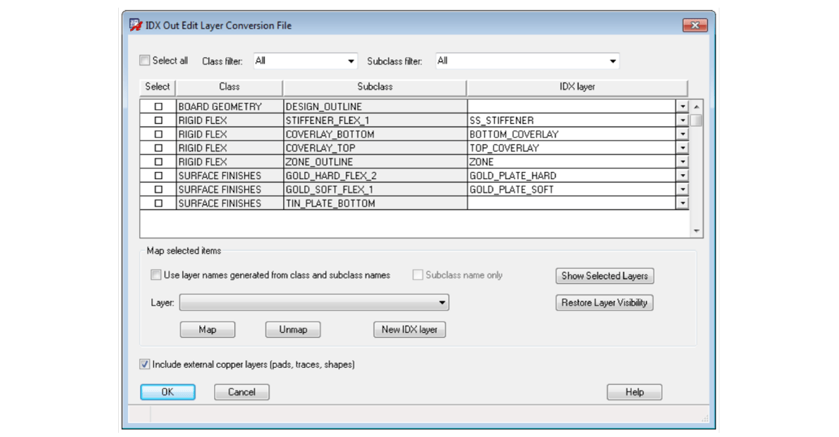
Since there are many different materials and different rules a PCB designer needs to deal with, enabling and specifying rules for the combination of layers should be intuitive and easy. A simple step-by-step process (Figure 6) involves:
- Selecting the layer by choosing the desired checkbox in the layer matrix
- Selecting the rule
- Setting the value
- Defining a label that means something to the designer
- Setting the DRC display layer
- Adding a description for the rule (rules should be preserved in the tool)
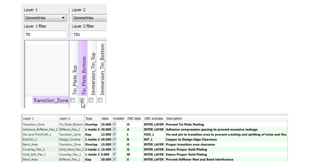
Users should be able to run inter-layer checks online or offline and in batch mode. When running the checks online, the user simply sets the rules and should be able to run the DRC and view DRC results.
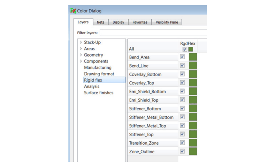
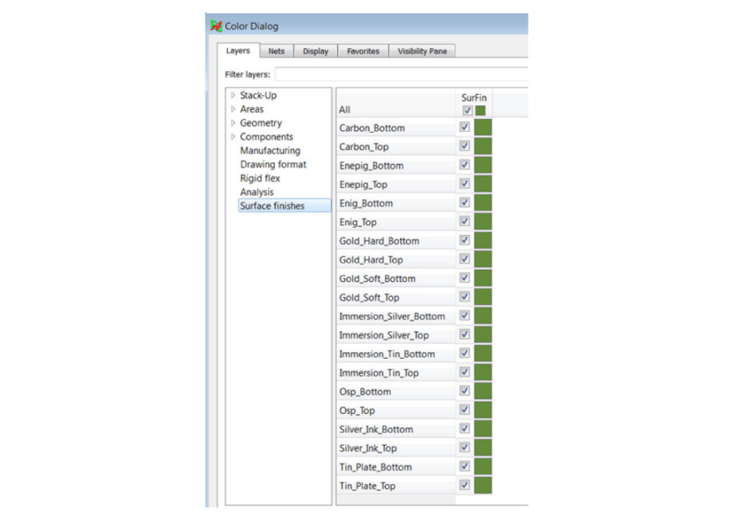
Most EDA tools have long supported rigid-flex PCB designs. Ideally, the latest versions of these tools need to address new challenges stemming from multiple board layers, while providing a wide breadth and depth of in-design checks covering more than 30 new native flex and surface finishes layers (Figures 7 and 8). Users should also be able to incorporate their own layers for the tool to check, so they don’t have to wait for tool updates.
Cadence’s Allegro 17.2 PCB design portfolio automates inter-layer, in-design checks in rigid-flex PCBs, providing the capabilities discussed in this section. By allowing you to perform DRCs for various non-electrical flex layers, the tool helps to save time and avoid respins. The tool also supports real-time concurrent team design, so multiple PCB designers can work on the same PCB design database.
How much time a PCB designer can save using the rigid-flex design capability versus performing manual DRCs (and going through iterations with the fabricator) is proportional to the complexity of the design. Aside from time savings, another benefit from using the capability is the ability to prevent omissions or other errors that could impact PCB design quality and overall cost. After all, problems that are discovered by the fabricator will naturally be more costly and time consuming to resolve due to the rework and iterations needed.
Data Transfer to Manufacturing
Rigid-flex designs are unique when transferring the design data to the fabrication process. The various build-up of materials that make up the final product must be clearly defined. Identification of the various materials and correct order that define the layer structure must also be identified for each zone through proper documentation, or through intelligent manufacturing data formats (see Table 1). Failure to provide proper detailed information may result in costly delays or incorrect results of a final product. Communication with the fabricators to identify their requirements is key to a problem-free process.
| Multiple Stackup Table | ||||||
|---|---|---|---|---|---|---|
| Units = Microns | ||||||
| Name | Type | Material | Primary | Zone 1 | Zone 2 | Zone 3 |
| Stiffener | Mask | Stainless Steel | 200 | |||
| Adhesive | Mask | Thermoset | 55 | |||
| EMI Shield | Mask | EMI Shield | 22 | |||
Design houses and fabricators agree on a stack-up for a design that has impedance control or flex/rigid-flex designs because of the complexities involved. Traditionally, design houses and their fabrication partners use spreadsheets, presentations, and other such tools to communicate build intent. These methods are both time-consuming and error-prone. To avoid such problems and save time, advanced PCB designers now use IPC-2581 to exchange stack-up data electronically. IPC-2581 is an open, intelligent, neutral design data exchange format that is supported by over 85 PCB design and supply-chain companies worldwide. IPC-2581 revision B now supports bi-directional exchange of stack-up data to eliminate discovery of problems late in the design hand-off cycle.
Summary
Rigid-flex PCBs provide a reliable and flexible option for meeting the small form factor and low weight requirements of a variety of applications. However, as flexible technology has evolved, new design challenges have cropped up. PCB design technology that automates the detection of errors as they are made through in-design inter-layer checks in rigid-flex PCBs can help meet these challenges, helping you deliver a quality product within the desirable time-to-market window.