White Paper
3D Connection Artifacts in PDN Measurements
Overview
Introduction
Milliohm impedance can be measured with vector network analyzers using a two-port shunt-through connection. Typical Devices Under Test (DUTs) not having coaxial connection to the DUT's rail require probes connecting to the test site [1] [2] [3]. Probe connections unfortunately create a small open structure where the probe pins meet the DUT. Using two probes connecting nominally to the same DUT location, the crosstalk/coupling between the probe tip loops will alter the results. Connecting to a DUT with two probes can be best done at test-via pairs connecting from opposite sides of the DUT. One-piece two-port probes simplify the manual handling of probes [4]. When the two ports are in close proximity, the coupling between the probe tip loops can be de-embedded or calibrated out based on its equivalent circuit. DUTs with through hole pairs connecting power rails offer the flexibility that we can either use probes attached to the DUT from opposite sides (to reduce probe-tip coupling effects) or probe the DUT from the same side and de-embed or calibrate the probe-tip coupling. Some DUTs do not offer this flexibility. For instance, measuring the PDN impedance in large pin-fields, where one or both sides of the supply rail use only blind vias or one side is inaccessible due to mechanical constraints, requires same-side probing [5].
Calibration and de-embedding options have been reported in [1] [2] [3] [4]. Calibrating to the tips of probes may remove part or all the probe-tip coupling error, but it still leaves in place the effect of coupling between the via-trace structures that lead from the landing points to the planes further down in the stack-up. It must be noted that the de-embedding or S>>Z>>T transformations require the full two-port S parameters and carry the concern that we are using S11 and S22 from the measured results, which we know can be inaccurate. If our goal is correlation at the surface connections, including the DUT traces/vias connecting to the planes, we have an additional challenge: large boards and sophisticated packages can be simulated faster and with less computing resources with hybrid field solvers, which capture the modal resonances of planes accurately but use approximations for local details, such as vias, pads, and anti-pads. In this paper, we will capture these via coupling and trace coupling effects in simulation using hybrid EM solvers and full-wave solvers. We will analyze probe-via coupling and its removal by de-embedding/calibration. Multiple DUTs will be investigated, starting with simple test boards that can be easier to analyze and connect to. More sophisticated DUT boards [5] are also used to look at the parasitic probe-via coupling in two-port shunt-through self and transfer impedance PDN measurements.
1. Two Port Shunt-Through Measurements
Measuring impedance using a single port is only accurate for impedances above 1Ω [6] due to load-to-port mismatch and parasitic of launch masking lower impedances. To get around this issue, we use a two-port shunt-through measurement [7] [8]. Figure 1 shows the two-port technique where port 1 drives the current through the DUT, and port 2 measures the voltage.
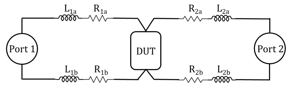
Looking in from Port 1, we see the low impedance of the DUT in parallel with the 50 Ω of Port 2. The reflection coefficient is nearly -1.
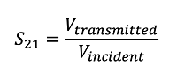
Since the magnitude of the current through the incident loop is Vincident/50Ω, and there is an equal amount of current from the reflected signal, we see that
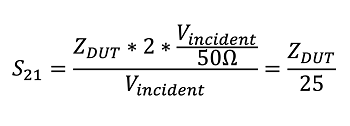
In this way, we see that using two ports to obtain S21 will give us a much more accurate measurement of the low impedance of the DUT power rails, also because transmission measurements tend to have a higher dynamic range than reflection measurements.
We can also extract the Z matrix from the S-parameters and convert this to a more convenient description of the DUT, converting in a T equivalent circuit, as explained in [3]. Figure 2 shows this process.
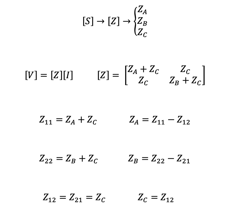
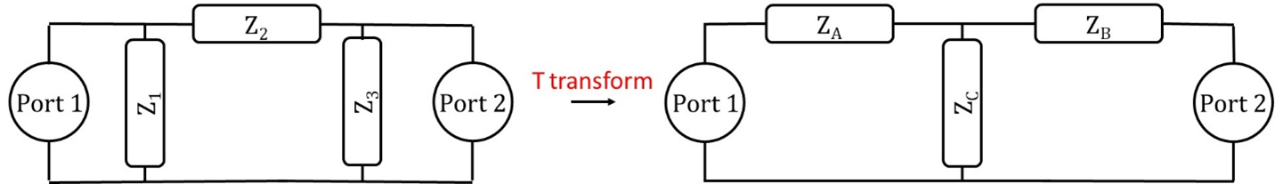
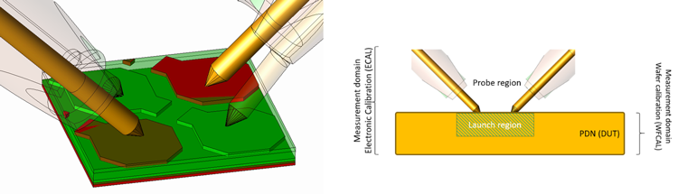
Note that the Z11 and Z22, as well as the extracted T equivalent circuit, require the use of S11 and S22 measurements that tend to have limited accuracy and dynamic range. This is further discussed in the following section. To support the analysis, it is useful to look at Figure 5 and Figure 6 that show the physical placement of the VNA probes. The probes form a 45° angle with the board surface.
Although the coupling between the two probes at ports 1 and 2 can be removed by calibration, there will still be coupling to the via-trace structures in the board. The T-circuit transformation provides a convenient way of eliminating the probe series parasitic to derive the shunt element ZC, which represents the DUT. However, as was shown in [9], the actual ZC term is impacted by mutual coupling within the PCB launch area. Simply having two orthogonal loops does not guarantee zero magnetic coupling. The magnetic coupling can be minimized if there is also symmetry. To minimize both electric and magnetic coupling, full symmetry is required (Figure 3 top right illustrates these three scenarios with the top views of two via loops).
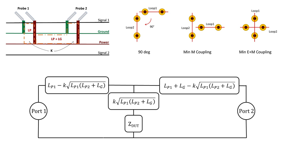
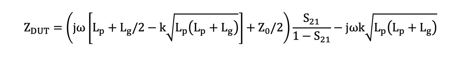
In Figure 3, LP is assumed to be the inductance of the power/ground via pairs extending the physical probes, and both launches are assumed to be identical with a coupling of k between the via current loops. LG represents the plane inductance between the launch vias. Thus, the ZC we derive is no longer only representing the PDN. There is a term folding into ZC stemming from the via coupling where the system is probed. That is equivalent to saying that the error in predicting ZDUT grows with frequency that could very well mask the actual DUT. Therefore, we would expect this term to be very important when measuring low impedance power delivery networks. To truly get the ZDUT in Figure 3, we would have to remove this term. Reference [8] shows the mathematical relation connecting ZDUT with S21 and the parasitics from the probe launch. The equation is repeated below:
Although this equation can be simplified to
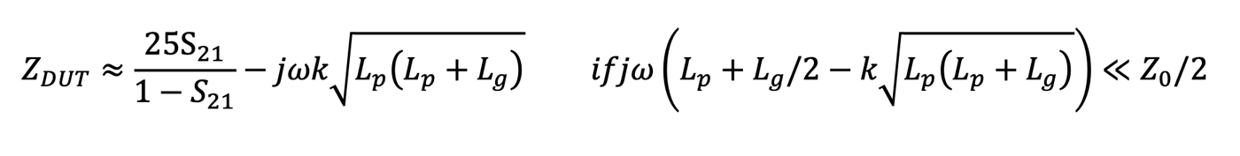
we are still left with the challenge of finding the different inductive terms and their coupling coefficient. The error can be minimized by reducing the distance between the probe points (minimizes LG) and putting the probing vias within the PCB close (minimizes LP) – the error is simply scaling with ωkLP. By doing so, we are maximizing the contribution from the coupling between the actual probes, a term that itself creates a parasitic that will fold into the extracted DUT impedance as discussed above.
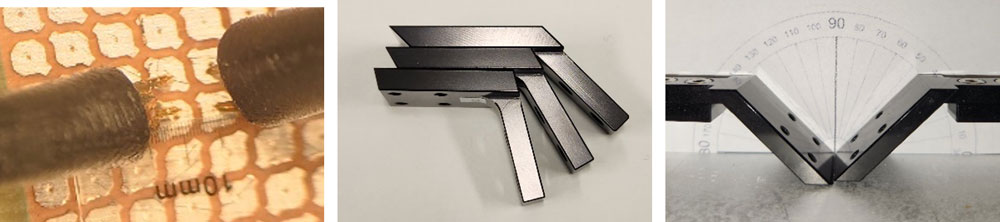
Separating these very small impedances is a non-trivial task, so let’s try to think of this setup in a different way. We know that the two-port shunt through measurement technique is good for removing parasitics that are in series with the probes. Can we transfer the coupling terms within the PCB from a series DUT contribution to a series probe contribution? Can we see the via and pad structures where the probe tips land as an extension of the probes themselves? In so doing, it would effectively push the calibration plane down into the first layer of the PCB PDN cavity. The de-embedding technique proposed in IEEE P370 could be used to accomplish this task, if not for one important point: for power delivery, most high performance BGA power pin-outs employ a checkerboard pattern, which means that the pins are anti-symmetric, as shown in Figure 4, while P370 requires that the structure be symmetric for the de-embedding to work properly.
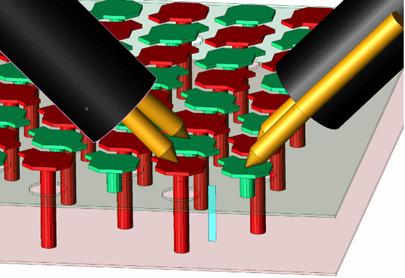
The method we will attempt to implement in this paper is instead to see the launch as a series extension of the DUT. That is, we will de-embed from the probe pads to a port exactly between the pads (the blue vertical rectangle in Figure 4). The de-embedding will be done using an extracted model of the launch structure.
The method will not change how we probe or calibrate in the lab but would add a post-processing step where we remove PCB launch parasitics using an extracted S-parameter model. The methodology creates several challenges related to ensuring that the extracted PCB launch model properly represents what is being measured in the lab, not least is that the model is dependent on probe angle, spacing, offset, probe orientation (Figure 7) as well as the measurement environment. Thus, it would be preferable to find a parameterized model of the launch taking into consideration these variables rather than having separate extractions for each probe configuration. In addition, there are some unknowns in relation to following the methodology for PDNs with more than one power/ground cavity. Finally, parameter sensitivity should also be investigated. These challenges are not pursued in this paper and they would make for some interesting future investigations; in this paper, we will focus on the general method.
1.1 Devices under test
1.1.1 Solid copper sheet
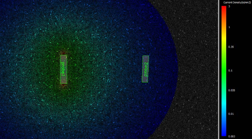
To minimize the number of variables, the tests started with the wafer probes landed on a rectangular piece of solid copper sheet (see section 3.3 for data). The size of the pure sheet is approximately 15.6x31.5 mm with a thickness of 0.25mm. The size of the sheet is big enough that when we land two probes on it in close proximity, we can consider the sheet as having infinite horizontal dimensions. Between two contact points, the resistance of the sheet can be calculated from analytic expressions [10]. Figure 5 shows the photo of the full copper sheet, a close-up with two probes landed and a simplified equivalent circuit.
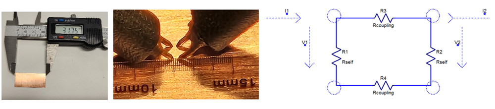
Note that this setup stresses the measurement in two ways: not only do we need to measure low impedances at both probes, but also the connection between the two probes stresses the cable-braid loop mitigation solution.
1.1.2 Test board with 8x8 via arrays
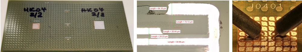
The test board has 20 layers and 5 power-ground cavities. In one section of the board, there are four blind-via arrays and two through-hole arrays. The blind-via arrays were cut away from the rest of the board. The cut piece (on the left of Figure 6) was measured at the right via array (J0401), which connects the second and third layers (stack-up dimensions shown in the middle photo of Figure 6). The inductance of the structure was measured by looking at the impedance at the center of J0401 via array (right photo) while the entire area of the J0400 via array was shorted with a copper sheet.
Note that the via array has a checkerboard pattern alternating power and ground connections, which requires the probes to be in opposite orientations (called “flipped” in this paper) facing each other with no offset.
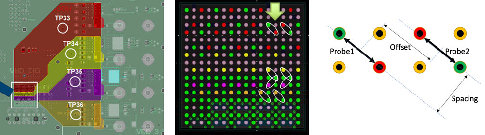
1.1.3 Customer demonstration board with 1mm BGA via field
The SI and PI challenges and solutions of a 12-layer demonstration board for a high-speed chip are shown in [5]. During the original work, the measurement-simulation correlation of the power rail inductance in the chip’s pin-field exhibited poor correlation, primarily due to the limited probing capability that was available for the project. Figure 7 shows the geometry of planes, the 1mm BGA pin-field with the four power-ground pads where the impedance is looked at highlighted by the large green arrow (middle insert). Note that the two probes need not only to be flipped, but they are also offset, so that the four contact points form a rhomboid instead of a rectangle (illustrated on the right).
2. Simulating Low-Impedance PDN Configurations
Extracting models of low impedance configurations naturally requires consideration of all parameters that go into the extraction tool as well as the actual extraction method. Starting with the obvious—the input data must describe sufficiently accurately what is being measured in the lab. Stack-up parameters such as thicknesses should be adjusted along with process parameters such as plating thickness and material properties properly calibrated (specifically, conductor electrical conductivity and dielectric constant).
The most appropriate extraction methodology must be chosen. Today, a majority of PDN simulations are done in hybrid EM simulation environments like [11]. The hybrid methods decompose the board behavior into plane modes, transmission line modes, and localized discontinuity models like vias and padstacks. Decomposition makes the extraction very fast and is capable of handling even the most complex board layouts being designed today. Very good correlation has been achieved for many different PDN investigations, including [12]. However, when studying very detailed and localized behavior, typically around field transition areas, the user must be careful with solvers that use the hybrid method and should correlate results in a full-wave 3D electromagnetic extraction. This present work is primarily concerned with the frequency range on a PCB where sub-mΩ resistance may be achieved and thus where the local distribution of currents is a key in understanding the realized resistance. Users must also be careful applying typical full-wave 3D solvers, as these normally apply skin impedance boundary conditions and other higher frequency-oriented settings. The transition from bulk current conduction mode to the skin depth dominated conduction mode is of key importance to the accuracy of the simulation, and a volume mesh for the conductors may be required to properly resolve the redistribution of currents as we go from the very low-frequency behavior towards the skin depth dominated region. For typical frequencies and conductivities used in electronics the skin depth, δ, can be expressed simply as
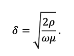
Generally stated, when the frequency is below where the thickness of the conductor is smaller than twice the skin depth, we have bulk current conduction. As we move from the frequency where the conductor is 2δ to 5δ we see a gradual separation of currents on the top and bottom layers of the conductor until eventually at 5δ thickness the current flows are purely following a relationship.
Figure 8 shows the 2δ and 5δ limits for a pure copper conductor (58MS/m) in the thickness range typical for PCB applications:
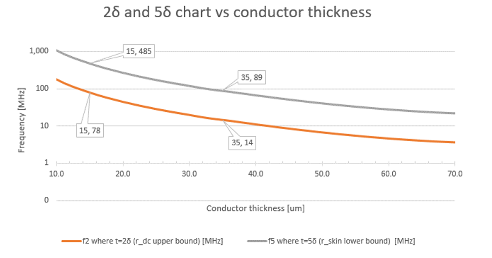
We see that for metal with an approximate thickness of 35μm the transition region is 75MHz wide and happens right in the range where you expect the PCB PDN to deliver low impedance. The effect of the lower copper conductivity in processed PCBs is to widen the transition band. For example, with a PCB copper conductivity of 46 MS/m, the transition band extends to 94MHz for a conductor thickness of 35μm. The 2δ limit in this case is raised from 14 to 18MHz. Typically, 10MHz is quoted as a lower limit for full-wave FEM solvers, below which the full-wave solvers become unstable. This is important to keep in mind when looking at the bulk current conduction region. There are typically two alternative paths to follow in that region. One option is that some full-wave FEM implementations apply specialized solvers in this region as well as a detailed volumetric mesh to capture current redistribution through the conductor. Alternatively, a quasi-static solver could be used. In either case, careful consideration of meshing and convergence studies is required. Finally, the user should be careful with the field solver convergence settings, and several convergence studies should be done for the field solver of choice.
The importance of understanding the exact behavior at DC started out with the first calibration measurements we did on the solid copper sheet. Counterintuitively, we found that the transfer resistance lowered as we moved the probes away from each other. This was initially puzzling behavior – we had expected the resistance to increase between probe points as we separated the probes. However, that is not what the ZC plot was showing in the measurements. To understand the result, we should consider in detail what Z21 actually represents, along with rethinking our measurement setup to fully appreciate what ZC is indicating.
When measuring transfer impedance using the two-port method for a low impedance DUT, as shown in Figure 3, Z21 is the voltage measured on port 2 with current only flowing in through port 1.
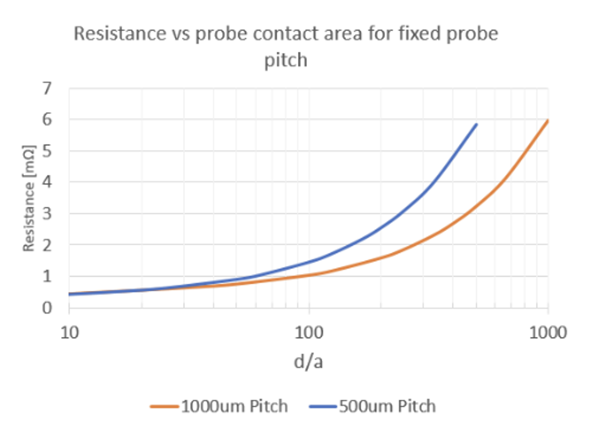
Only a tiny fraction of the injected current from port1 flows into port2 since the probe impedance is much larger than the plane resistance between the two probe tips. However, the plane current density induced by port1 causes a voltage drop over the area spanned by the probe tips of port2. The effective resistance between the probe tips on port2 is a function of the pin spacing and remains fixed if we do not change probes (assuming we keep the contact surface identical). As is to be expected, the plane current density caused by port1 scales with 1/d2 and thus, we would expect the voltage sensed by port2 to scale in the same way. This explains the lower transfer resistance as we move the ports further away. This intuition is confirmed in reference [9], which provides an analytical calculation for the resistance between two points with a finite contact area and distance. First and foremost, the main point was to develop an intuitive understanding of the results. For reference, the resistance between the tips of a 1 mm pitch probe is roughly 0.77mΩ with the contact radius being 1/50 of the pitch, i.e., 20μm contact area radius. Maintaining the contact area but decreasing the probe pitch to 500μm, the resistance will be 0.63mΩ [9]. This calculation assumes infinite plane size, which is obviously not the case for the practical board measurements. The contact resistance is expected to be larger in the practical case. Further discussion is provided in section 4.1.
2.1 Sensitivity Analysis
When simulating impedances in the µΩ range, the results can be very sensitive to a variety of physical parameters. Performing sensitivity analysis helps the engineer understand which parameters will have the biggest impact on the results. The knowledge acquired can help the engineer understand which parameters are most critical for getting valid measurements. In this paper, we show results from a small sensitivity analysis exercise. A more detailed sensitivity analysis study is beyond the scope of this work.
When looking at the structure of the probes on a shorting sheet of metal, we realize there are three key parameters that can be changed that will have a profound effect on the DC resistance of the simulated structure:
-
 The sheet thickness (TH). At DC, the current will more easily redistribute and use all the copper thickness available, so it will not be the same for a 10, 20, or 50mil thick copper sheet.
 - How deep the probe goes into the metal (probe offset, OFF). The contact between the probe and the sheet presents a current crowding point. We know all the current has to go through there, so any increased resistance in that section will directly impact the measured DC resistance of the whole structure.
- Surface roughness of copper (SR).
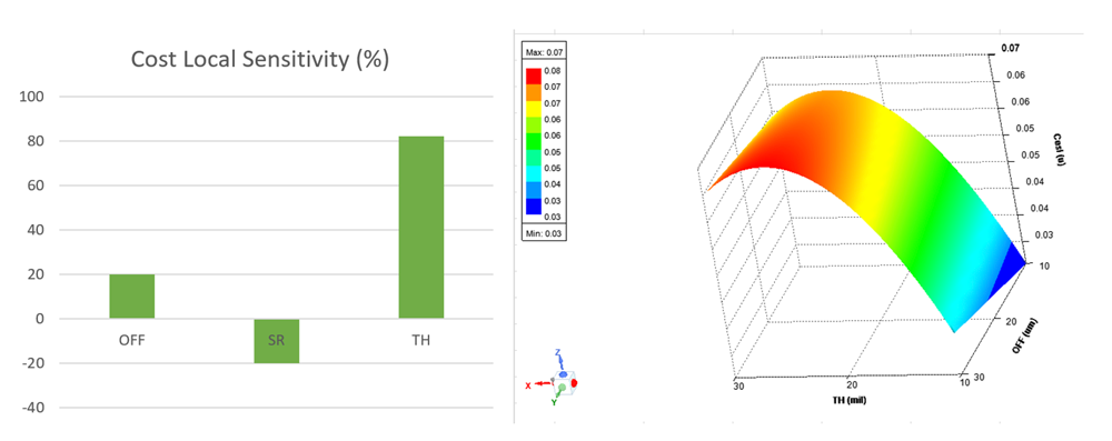
To determine the best fitting of these variables to get a good match to our measurement results at DC, we ran a Design-of-Experiment [13] with the identified variables. Sheet thickness was adjusted from 10 to 23mil, probe offset adjusted from 10 to 30µm, and finally a Hurray SR model for surface roughness with a nodule radius between 2 and 6µm.
The optimization is minimizing the following cost function expression where 0.407mΩ is the value of the straight probe orientation impedance at 100Hz. The smaller the cost function, the closer our simulation results are to measurements.

From the results in Figure 11, we see that the metal sheet thickness has the highest sensitivity with a maximum sensitivity at the mid-point of the range of thicknesses. The probe offset and surface roughness have approximately the same sensitivity, and both show little contribution to the low frequency impedance. The minimum value of the cost function happens with the following parameters: thickness 10mils (min. of the range), probe offset = 10µm (probe barely touching), and surface roughness 6µm (maximum).
3. Measurement Considerations
The connection geometry to the DUT shown in Figure 4 brings up practical challenges, constraints, and limitations both in simulations and measurements. In this chapter, we look at these and some of the possible solutions in the measurement space.
3.1 The instrumentation
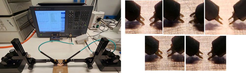
Frequency-domain power distribution measurements are typically done either by measuring the self or transfer impedance of the DUT or by measuring voltage transfer functions on filtering circuits. Impedance measurements can be done using a vector network analyzer (VNA) or a frequency response analyzer (FRA), whereas voltage transfer measurements of filters are best done with FRAs. In this paper, we focus on board PDN impedance, and though some tests have been done up to 3GHz, many of the low-frequency measurements also offer important and interesting learning. To allow us to look at low impedances at low frequencies, a VNA model with low-frequency extension [14] was used. VNAs can measure low impedance in a two-port shunt-through configuration [8], but we need to be careful to suppress the low-frequency error created by the loop formed by the two cable shields. Many techniques exist to reduce or eliminate the cable braid loop error, but still, it is a good idea to minimize the cable braid error to start with. This can be done by minimizing the cable length and/or by selecting cables with low shield resistance, while maintaining good cable flexibility. To meet these requirements, for measurements in the 100Hz – 10MHz range, two half-meter-long PDN cables were used to connect the VNA to the probes [15]. As shown on the left photo in Figure 12, this length was a comfortable minimum to reach from the VNA to the probes and these cables have low braid resistance and are also very flexible.
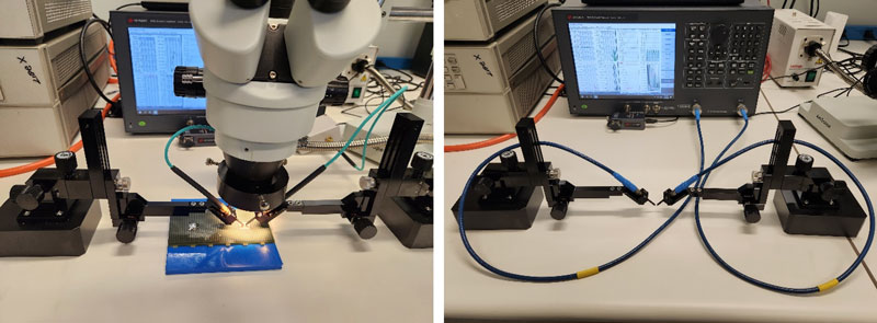
To further reduce the low-frequency cable-braid error, a common-mode choke was used, which is also available commercially [16], but to achieve the highest possible dynamic range, a home-made toroid common-mode choke was created for our setup using a nano-crystalline alloy core [17]. When the measurements extend to the GHz frequency range, the DC resistance of the cable braid matters much less, and therefore, in the setup covering the 2MHz – 3GHz range, we used high-frequency cables [18]. The proper choice of probes depends on the DUT and frequency range. Probing printed circuit boards for PDN measurements requires robustness and not necessarily a very high bandwidth [19]. These single-ended probes have a symmetric construction, allowing us to use the same piece for either G-S or S-G probe configuration. To perform calibration, we had two options: a) to calibrate to the end of the coax cables with an electronic calibration kit [20] and b) calibrate to the tips of the probes with a wafer-probe calibration substrate [21]. These instrumentation options are shown in Figure 12. Note that while it would be more convenient to use only one connection scheme, for practical reasons it would be too hard to achieve both goals simultaneously: solutions to mitigate the low-frequency cable braid loop are not particularly good at high frequencies, and vice versa: cables with good shielding effectiveness and good stability at high frequencies do not necessarily have low DC resistance.
3.2 The test setup
Figure 13 illustrates the low end of the dynamic range of the chosen low-frequency setup. After full two-port calibration to the end of coax cables, a reference piece was measured: a pair of back-to-back female SMA connectors with the center pins shorted to the frame with a solid copper sheet. When we measure this piece without the common-mode choke, at low frequencies we get the blue trace, corresponding to the DC resistance of the two cable braids in parallel. When the common-mode choke is in place, we get the green response, which is still approximately 3x (~10dB) above the noise floor, shown by the red trace. The red trace is obtained with the ends of coax cables terminated but not connected together.
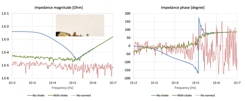
With a common-mode choke, this is the low end of the dynamic range available to us. We also notice that the phase of the measured impedance is negative as we approach 100Hz. This is the residual error due to the finite inductance of the common-mode choke. We could eliminate this remaining error, too, using a DC-coupled isolation amplifier with high common-mode rejection. However, this would prevent us from doing full two-port calibration to the end of coax cables, so we would need to characterize the amplifier separately and de-embed it from the test result. Another method would be to use Enhanced-Response-Through calibration with the amplifier setup, which would be sufficient for measuring only the shunt element of the DUT complex. When we also need the transfer parameters, we need the full S-parameter matrix, which could be obtained by swapping the cable connections and remeasure the DUT in the opposite direction as well. In our setup we cannot use this option because the coax cables have to be attached to the probes: we cannot swap the cables while the probes are landed, and if we lift the probes, we cannot guarantee to land again on the same exact location. In contrast, the common-mode choke is a reciprocal passive device, allowing us to use full two port calibrations to the end of coax cables or to the tip of the probes with wafer calibration substrates.
A question remains: where to place the common-mode choke; in the path of port1 or port2. To determine its optimum location, we have to consider the DC and AC bias sensitivity of the choke. The question about DC (current) bias sensitivity can be eliminated by restricting us to measure only unpowered boards, so no DC current will flow through the choke. Ferromagnetic materials with very high permeability are also sensitive to AC bias, which influences the inductance. Though we don’t need to count on an accurate inductance from the common-mode choke, if the AC bias reduces the inductance significantly, it would reduce the effectiveness of the choke, resulting in higher residual error. In this respect, we can use two things: if we use an electronic calibration unit, those typically require -10 dBm or even lower source power. For the unit we used, -15dBm was recommended, which is low enough that we don’t see a reduction of inductance due to AC bias. However, after calibration, we need to increase the source power to the maximum +10dBm, otherwise the noise floor would be high. Luckily, we can keep the AC bias very low across the common-mode choke if we place it on port2, which gets only very small signals when we measure low impedances.
Note that some impedance plots in this paper stop at 10MHz, because the common-mode choke’s construction introduces resonances above 30MHz. If we need to cover a much wider bandwidth beyond what the common-mode choke could cover, multiple setups and connections become necessary (as shown in Figure 12) and we need to stitch the results together from separate measurements; we can see this on the two red traces on the right plot in Figure 26.
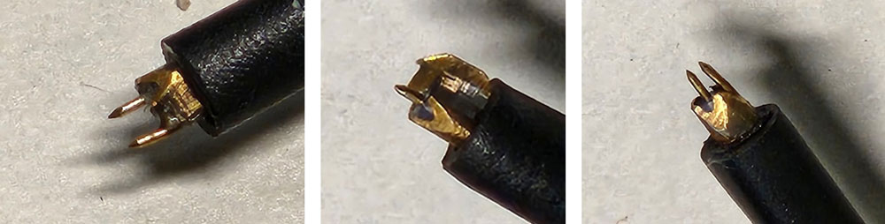
Using two single-ended two-pin-per-probe wafer probes for our measurements, we also need to ensure proper landing of all four pins on the DUT, see Figure 14.
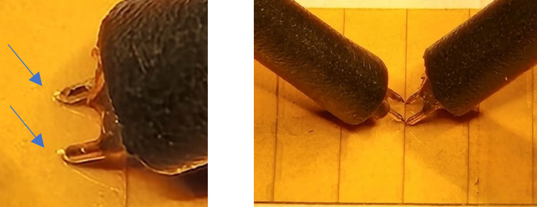
As we will see later, the coupling between the probe-tip loops makes the setup very sensitive to even small changes in the geometry and therefore we need to align the two probes as much as possible. This can be done by first planarizing the probes, making sure that both tips touch down simultaneously, and by aligning the tips to be parallel, which can best be done by using the mylar sheet supplied with the probes. The left of Figure 14 shows planarization. Notice the tiny bright spots next to the probe tips (highlighted by the arrows); these indicate touchdown by capturing the deflection of light as the probe tip pushes into the soft polyimide surface. We achieved good planarization when these bright spots were symmetric and showed up at the same time as we moved the probes downward.
We will also see later that the size of the open loop formed by the probe tips has a direct relation to the spurious coupling between adjacent probes. To illustrate this effect and to measure DUTs with different pad pitch, three different probes were investigated: 1mm-pitch probes with pins, 1mm-pitch probes with ground blades, and 0.5mm-pitch probes with pins. Close-up photos in the above order, left to right, are shown in Figure 15.
In addition to keeping the probe contacts parallel, the probe spacing and the landing angle are also important to set and/or measure accurately (see Figure 16). To assist this using the optical microscope we had in the setup, a transparent microscope ‘ruler’ was used, which allowed us to determine the distances with approximately ± 50 µm resolution. The probe-tip coupling values also depend on the landing angle of the two probes: for a given horizontal spacing, the steeper the landing angle, the tighter the coupling becomes. The probes used for these tests have adaptors available to set different landing angles. Considering the shape of probes near the tip, the lowest landing angle is limited to approximately 30⁰. The diameter of the protection sleeve on the probes, as well as the optical vision system we currently use, limited our choice of the landing angle to a single value, 45⁰. Additional landing angles are planned to be investigated later with a different vision system.
3.3 Reference measurements
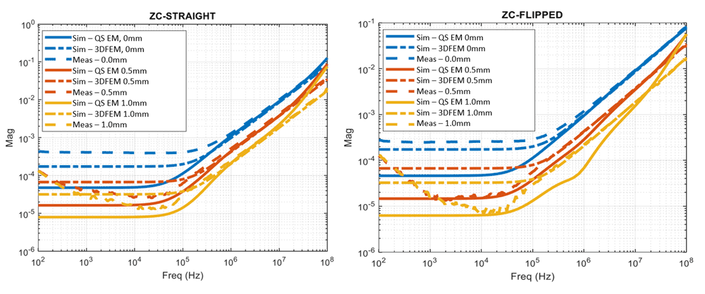
To assist the correlation work on more complex DUT structures, simple tests were performed where the number of variables was kept at the minimum. The DUT was a solid sheet of pure copper. When very low impedance is measured, it may be hard to determine whether the probe landing is correct or not. With the probes used in this study, we have four somewhat rigid tips to land on the DUT. There are several possible combinations of how we can land incorrectly four pins. Some of these incorrect landings are easy to detect in the results: for instance, when the two signal pins are landed properly, but if one or both ground pins do not make a good connection, we get a high impedance value, which is easy to detect. It is harder to detect cases when one or both signal pins are not landed properly, especially when the correct data is close to the noise floor. Under such circumstances the coupling between the probe pin loops can help us to identify the issue. Figure 17 shows the setup and probe close-ups of two correct landing geometries and three incorrect landings. The two 1mm pitch probes had a fixed 1mm horizontal separation. The two correct landing cases are when the two probes are connecting straight (meaning that the signal pin is across signal pin and the ground pin is across ground pin) and when the signal pins are across ground pins (called “flipped”). The three incorrect landing cases are when none of the four tips makes contact, when the signal pin of probe1 is not making contact, and when the signal pin of probe2 is not making contact. The measured data is shown in Figure 18 (showing the impedance magnitude and phase) and Figure 19 (showing the resistance and inductance).
We can make the following observations. The complex impedance values were calculated with the generic S21/(1-S21) formula, which yields self-impedance if the two probes are connected to the same location. Here, however, the four landing points were at the corners of a 1 mm square. The distance between two landing points belonging to the same probe (either port1 or port2) determines the impedance between those two points, which could be considered as self-impedance. With our geometry, however, the spacing and therefore the impedance of the sheet between port1 and port2 probes is also the same as the self-impedance sensed by either probe, which creates a voltage attenuator between the two probes (Figure 5), and because of this, strictly speaking, the plotted impedance is the transfer impedance.
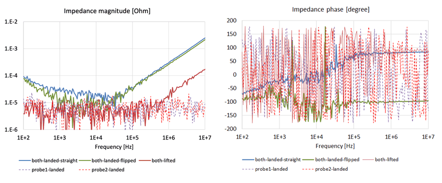
On the impedance magnitude plot the three incorrect landing cases are not identical. Below approximately 500kHz all three cases run mostly below 10µΩ, which is the noise floor of the given setup, but approaching 10MHz the ‘both-lifted’ case shows a rising impedance. This happens because when one of the two probes is correctly landed, it results in a short connection (either the transmit side is shorting, creating a very low voltage across the tips, or the receive port is shorted, shunting any stray signal pickup), but when all pins are floating, we have maximum voltage across the transmit pins and the small capacitive coupling to the (not shorted) receive pins will create a measurable signal. When all four pins are correctly landed, we see a downward-sloping response in the 100Hz - 1kHz frequency range. That is the residual error created by the cable braid loops, reduced but not completely suppressed by the common-mode transformer.
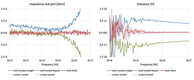
The real part of impedance and equivalent inductance show practically zero values when any of the four pins are not connected properly. With proper connection, the sign of impedance completely flips. With cross-connected (or flipped) probes both the real part of the impedance and the inductance becomes negative. This is important to keep in mind when we need to change the orientation of probe tips to match the geometry of the DUT.
Additional reference measurements were done by landing the three different types of probes on isolated shorted bars. This tells us about the mutual inductance between the probe tip loops without the need for a common-mode choke in the cabling. Measurements were done on a calibration substrate with 0.3mm, 0.5mm, 0.7mm, 1.0mm, and 1.5mm horizontal spacing.
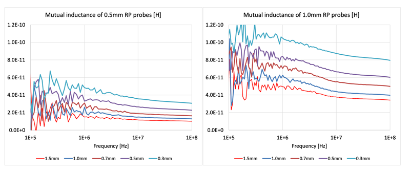
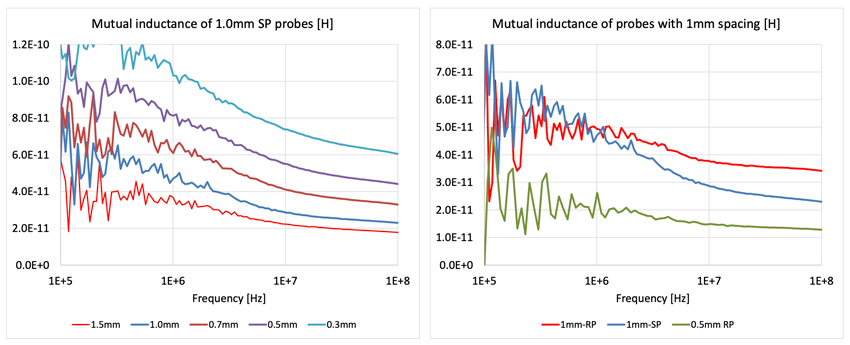
Note that the mutual inductance is proportional to the loop size, but it also depends on the tip geometry: For the same 1mm probe tip spacing, the blade construction has lower inductance at high frequencies but somewhat higher inductance below 1MHz.
4. Measurement to Simulation Correlation
4.1 Solid copper sheet
To determine how well we can extract the DUT impedance from our PROBE-DUT-PROBE measurement and simulation results, we look first at our correlation results for the shorted case on a piece of copper.
For these simulations, there are two probes on the top, with 1mm separation between signal and ground per probe. These probes have been created with a component model that can be fully parametrized. The probe conductor is Beryllium with a conductivity of 2.5x10⁷ Siemen/meter (43% of cooper). The shorting sheet of copper metal under the probes is 5mm x 5mm x 1oz. This shorting sheet will allow us to understand and correlate the circuit R and L. We are using a full-wave 3D solver [13] and a quasi-static solver [22]. For the quasi-static simulation, we defined four sources and one sink. Probes1 and 2 each had two sources on their center and ground rings. The sink was placed on the back of the solid copper sheet and was defined to have a uniform current. No surface roughness was included in the quasi-static solver simulations.
Figure 22 shows that the inductive correlation in the measured and simulated probe impedance is very similar across six permutations. Given that the probe impedance is not changing, the fact that all six results match suggests that the T-network extraction is being performed correctly. For the DUT impedances shown in Figure 23, there is a good correlation of the higher frequency inductive portion of the results and some mismatch at the lower frequencies.
4.2 Test board with via array
The test board was simulated using two different approaches: a Hybrid EM tool [11] and a 3D FEM simulator [23]. Two different port setups are used. In the first 3D FEM setup, ports are placed at the 3D connector models mimicking ECAL+ ports at the center between pads as indicated by the blue rectangle in Figure 4. The second setup mimics the wafer cal., with lumped ports placed at the pads where the probes land and a port at the center. Finally, a second wafer cal. equivalent was simulated with the Hybrid EM solver. The geometry was measured with all sites open and with selected sites shorted. Since the shorted site setup matches more what we expect from a PDN measurement, we will focus on those results. Figure 24 shows the frequency-dependent resistance and inductance derived from the simulations. The graphs show both R and L derived from the T-transformation DUT representation (ZC) as well as the values for the internal port. In addition, we show zoomed-in correlation of the ZC transformed data with the low-frequency measurement.
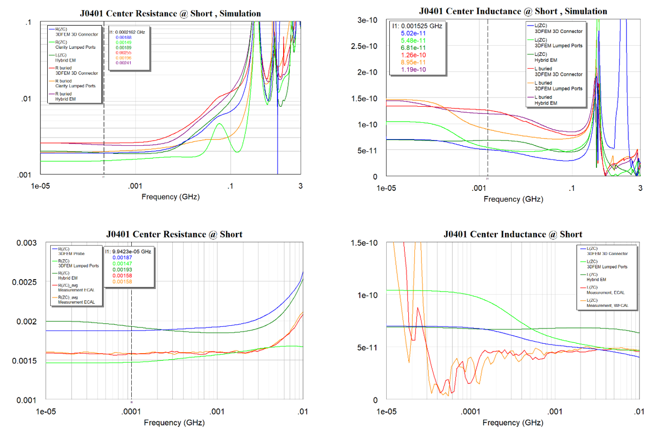
Starting with the correlation data in the lower frame of Figure 24, we see a reasonable agreement of resistance and inductance compared to the measurements. The effect of the DC isolation is visible in the inductance plot for the measurements. On the simulation side, we believe the differences seen in the 3DFEM simulations are coming from differences in convergence. This hypothesis will be confirmed by ongoing simulations.
We see that the low-frequency resistance in Figure 24 varies from 1.49 to 2.55mΩ depending on the extraction method and port location. The buried ports show slightly higher resistance compared to the external ports. Also, the lumped port extraction shows more frequency dependence just below 100MHz – again we expect that further refinement of the mesh is required to properly capture the transition from bulk current to skin depth dominated conduction. In addition, we see the impact of this effect in the inductance plots. The inductance extracted from ZC shows the lowest inductance, while the buried port is slightly higher. Overall, the simulations and measurement results agree well—provided you compare like for like, the buried ports should not be considered in such comparisons. Also, we note that the results from the different EM simulators agree quite well with the most variation in the inductive region and beyond. It is expected that the 3DFEM simulation with the full 3D probe models in place best represents the actual physical behavior because the coupling captured is physical. In contrast, placing lumped ports directly in the pads in the hybrid EM solver results in the possibility of coupling between the lumped ports because of their physical closeness. The hybrid EM is also expected to deviate due to the approximations in the transition regions. In this case, even in the setup with the actual 3D probe models we are making approximations since more effort is required to capture the loss profile of the coaxial cable connected to the probe.
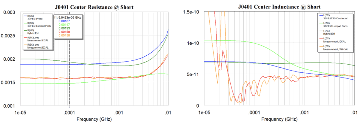
In Figure 25, we see that the measurements and simulations are well aligned up to 10MHz for both ECAL and wafer calibration, and these results align best with the 3DFEM analysis with lumped ports placed directly on the board. Measurements above 10MHz are in progress.
Notice that in this case ZC for both ECAL and wafer cal. agree, showing that in this case the coupling from probe to probe or probe to substrate is not influencing the results significantly. This is expected to change as we push to higher frequencies or are probing through vias in PDNs buried deep in the stack-up. Also, the present probe site has 1mm pitch which causes looser coupling compared to smaller pitch BGAs.
Now let us investigate transforming the measured data to see if we can get an agreement with the buried port results. For that we have extracted the launch region as shown in Figure 26.
To extract the launch region, a small piece of the board has been cut out which captures the parasitics in the launch region. In this case, the probes are included, allowing us to capture both the probe coupling and the launch on the PCB. In other words, this would be used with the ECAL data. A similar model could be created for the wafer calibrated data, and this model would then only contain the PCB launch region. Obviously, this would remove the entire cut-out region from the PDN, so some associated error is expected due to this process. We had anticipated that the parasitics of this launch could be mathematically removed from the measured data and that the resulting ZC would correlate to the buried probe impedance. Unfortunately, we discovered an issue, the process we had in mind requires 4 ports for the de-embedding to work and we only defined 3. Our initial thoughts to address this issue involved using a mode conversion block to create 4 ports from 3, but this caused an offset in the impedance curves. This topic is currently being investigated; one possible solution would be to define two buried ports back-to-back to create a 4-port network.
4.3 Customer demonstration board
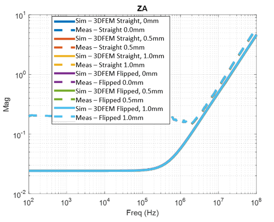
The board was measured in the BGA pin-field at the location that was identified in Figure 7. Note that in Figure 27, right side, the low and high frequency measurements with the Ecal unit overlap very well to the point that we cannot differentiate visually between the two sets of data. Also, the data measured with ECAL calibration lines up well with wafer-probe calibration with no isolation correction included. With ECAL calibration the reference plane is at the coax connection of the probe and both probes and the probe-tip coupling is included in the data. The good agreement with wafer-probe calibration without isolation calibration step illustrates and supports the claim that interconnect delay added in any of the two legs of the two-port shunt-through measurement outside the calibration loop does not noticeably change the result as long as the extra attenuation is low, and the added pieces are electrically short. When isolation correction is included, which removes the effect of probe tip coupling, we get higher inductance. This is due to the flipped orientation of the probes, where the loop coupling reduces the overall inductance.
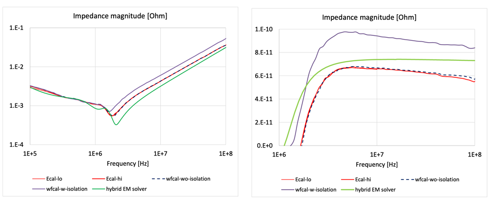
Note that the hybrid solver predicts inductance values, which are in between the measured data with and without isolation calibration in wafer-probe calibrations.
5. Conclusions
From a simulation stand-point, we have covered several important topics that users must consider in detail to get accurate low frequency simulation results. We investigated solver and mesh topics, variable sensitivity, and what to expect regarding the low frequency results. We showed that good correlation can be achieved between simulation and measurement for several cases. Using a simple copper sheet helped generate several learnings related to the behavior of the transfer impedance and plane current distribution. Finally, we have established a methodology for using simulation results to post-process measurements in order to remove coupling inherent in a launch structure from the two-port probe measurement methodology. Several points were highlighted in the paper where further investigations would be beneficial.
We achieved a substantial improvement in power-rail inductance correlation for a BGA pinfield by analyzing the contributors to the errors. During the work, we found that
- Electrically short delay outside the calibration loop does not noticeably change the result in two-port shunt-through impedance measurements.
- Typical probe-tip loop coupling inductance can be comparable to the laminate inductance in multi-layer PCBs and therefore the correct calibration or de-embedding of the probe-tip coupling is important.
- Probe spacing, offset, orientation, and landing angle all heavily influence the probe-tip coupling and therefore are all important parameters to be kept the same during calibration and measurements.
- The effect of probe-tip loop coupling can help to detect incorrect probe landing (shown in Figures 18 and 19).
- The isolation calibration step of the typical VNA calibration flow does not provide complete removal of the coupling effect.
The authors wish to thank the following individuals and companies for their help and support: Jin-Hyun Hwang, DuPont; Pete Pupalaikis, Nubis Communications; Steve Sandler, Picotest; Richard Zai, PacketMicro; and Graeme Ritchie, Cadence.
References
[1] B. Hostetler, "100uΩ Probing Methods," EDICON, 2018
[2] S. Sandler, "The Influence of Connectivity on Low Impedance Measurements," EDICON Online, 2021
[3] H. Barnes, "Modeling Passive Component for Power Integrity Simulations: How to measure, how to model, how to use," DesignCon, 2022
[4] Picotest, "Picotest P2102 two-port PDN probes," 2022. [Online].
[5] J.-R. Bonnefoy, T. Ballou, I. Novak, G. Blando, S. McMorrow and R. Mahadevan, "A Case Study in the Development of 112 Gbps-PAM4 Silicon and Connector Test Platform," DesignCon, 2021
[6] I. Novak and J. R. Miller, Frequency-Domain Characterization of Power Distribution Networks, Artech House, 2007
[7] L. Smith and E. Bogatin, Principles of Power Integrity for PDN Design Simplified, Prentice Hall, 2017.
[8] I. Novak, "Measuring MilliOhms and PicoHenrys in Power-Distribution Networks," in DesignCon, 2000
[9] V. Pandit, W. Ryu and M. Choi, Power Integrity for I/O Interfaces: With Signal IntegrityPower Integrity Co-Design, Prentice Hall, 2010
[10] S. Loyka, "A Simple Formula for the Ground Resistance Calculation," IEEE Trans. on Electromagnetic Compatability, vol. 41, no. 2, 1999
[11] Cadence Design Systems, "Sigrity PowerSI version 2022.1"
[12] M. Rotigni, "Reduction of the Conducted Emissions in Automotive Applications by Optimizing the Decoupling Capacitors," in CDNLive, Munich, 2016
[13] Ansys HFSS
[14] Vector Network Analyzer E5061B-3L5
[15] PDN cable
[16] J2102B Common Mode Transformer
[17] Toroid core data sheet, 3M or Amotech
[18] Sucoflex 100
[19] RP-GR-121510, RP-=GR-151505, SP-GR-181510
[20] Ecal N7550A
[21] Calibration substrate TCS50V2
[22] Ansys Q3D
[23] Cadence Design Systems, "Clarity3D, version 2022.1 HF3".
[24] Cadence Design Systems, "Clarity3D, version 2022.1"
[25] A. F. Angeles, H. Wang, W. H. Ryu and V. S. Pandit, Variables Affecting the Ultra-Low Impedance PDN Characterization, DesignCon, 2011