- Introduction
- Using Xtensa Processors to Accelerate Your Design
- Tensilica Instruction Extension (TIE) Language
- Performance Acceleration Techniques Using TIE
- Optimizing a Function: pop_count
- Customizing Storage—Adding a Register or Register File
- Adding I/O Interfaces to the Xtensa Processor
- Using TIE Intrinsics in C Programs
- Conclusion
- Additional Information
White Paper
TIE Language—The Fast Path to High-Performance Embedded SoC Processing
While using custom RTL accelerator blocks in data-intensive functions can provide high performance, they may require long design and verification cycle times. As an alternative, processor-based designs can reduce time-to-market and improve design flexibility while still achieving reasonable performance. Optimizing Cadence Tensilica Xtensa processors with new instructions and additional bandwidth using the Tensilica Instruction Extension (TIE) language enables you to compute and move data tens or hundreds of times faster than conventional processors, resulting in an SoC that is smaller, cheaper, faster, and consumes less energy. This white paper introduces the easy-to-use TIE language—which is similar to Verilog—as well as TIE techniques for accelerating computation and communication in an Xtensa processor.
Overview
Introduction
All processors do not yield similar performance for a particular application. A key differentiating factor among processor architectures is the number of operations that are issued and executed in parallel per clock cycle. Applied parallelism enables a processor to either complete more work at a given clock rate or complete a given amount of work at a reduced clock rate, improving efficiency. Most tasks contain a certain amount of parallelism, primarily dataand instruction-level parallelism.
Data-level parallelism, which allows the processor to apply the same operations to individual pieces of independent data, can easily be exploited by appropriate single-instruction, multiple-data (SIMD) function units. Instruction-level parallelism can be implemented through several architectural schemes that enable the processor to execute multiple operations at the same time. One way to simultaneously execute multiple independent instructions is to use a very long instruction word (VLIW) architecture that permits a compiler to encode multiple operations into one long instruction. Another way to execute multiple operations—usually dependent operations—in one clock cycle is to fuse the operations into one instruction. A multiply/accumulate (MAC), which fuses a multiplication operation with an addition operation, is a common version of a fused DSP operation.
Both computational and I/O operations benefit when designers exploit the parallelism inherent in most embedded tasks—and benefit even more when computational and I/O operations are combined. RTL hardware designers routinely exploit task parallelism with their hardware designs. However, many ASIC and SoC designers miss out on this opportunity because they regard processor IP as unchangeable, fixed blocks, as processor architectures historically required specially trained designers to develop custom-build processors that were tailored to be efficient for targeted applications.
The advent of customizable processor IP changes the game. A much broader range of designers—not just processor designers—can now develop processor IP that is tailored to specific tasks. These processors deliver the same or nearly the same level of performance as custom-built RTL blocks and offer several significant advantages.
Using Xtensa Processors to Accelerate Your Design
Optimizable Xtensa processors enable you to quickly develop extremely efficient function blocks for your SoC designs so you can:
-
 Future-proof your design—firmware is programmable to accommodate changes in requirements, specifications, and standards
 - Use an automated process to build the Xtensa processor, creating guaranteed correct-by-construction functionality
- Avoid lengthy RTL verification time
- Reduce energy consumption by reducing the overall task execution time
- Get a unique, custom, and proprietary processor that no one else can replicate—protecting your intellectual property
- Optimize using C, no assembly coding required
Customization creates a unique processor that quickly executes your target tasks while providing flexibility through firmware programmability. See the Ten Reasons to Optimize a Processor white paper for more details.
You can optimize Xtensa processors using a wide range of checkbox options, including hardware multipliers, dividers, and DSP function units. Clicking a box adds the desired functions and makes the appropriate changes to the software-development tools, simulation models, and processor hardware RTL.
In addition, there is an even more powerful way to optimize an Xtensa processor—through a processor-description language called Tensilica Instruction Extension (TIE). TIE is a simple way to make Xtensa processors more efficient, extending the functionality by defining custom execution units, register files, I/O interfaces, load/store instructions, and multi-issue instructions.
Tensilica Instruction Extension (TIE) Language
The easy-to-learn TIE language builds on familiar syntax to enable you to move data significantly faster than conventional processors, resulting in a more efficient and less expensive SoC that consumes less energy. With a few lines of TIE, you can make a dramatic difference in the Xtensa processor’s performance and flexibility for targeted tasks:
- Create new instructions to increase processor performance and efficiency
- Reduce bandwidth of standard size transfers—define the exact data width needed for your application
- Fusion—merge serial operations into a single instruction that can be issued back-to-back to achieve single cycle throughput
-
- Exploit data-level parallelism
- Create SIMD registers and operations, and perform the same operation across multiple elements of a vector word
-
- Exploit instruction-level parallelism
- Create multi-operation instructions using the Xtensa Flexible Length Instruction eXtensions (FLIX)—a multi-issue VLIW with variable slot widths
-
- Increase data bandwidth—connect to RTL blocks, memories, or other processors via custom processor interfaces without going through the system bus, reducing I/O bottlenecks and improving data throughput
- Ports (general-purpose I/O, or GPIO) for point-to-point direct connections without flow control
- – Queue (FIFO) interfaces for point-to-point data transfers that require flow control
- Memory lookup interfaces to connect to arbitrary-width memories or RTL blocks for low-latency data transfers
-
You will find that TIE is easy to learn—its syntax is a mixture of Verilog, a hardware description language (HDL), and the C programming language. You do not need to worry about pipelining, control/bypass logic, and interfacing to other processor modules as the instruction extensions you define are integrated directly into the Xtensa processor pipeline. Note that TIE is used only for adding instruction extensions and datapaths to an Xtensa processor pipeline—it is not a general-purpose hardware design language.
The Xtensa processor supports a variety of extensions, such as single- and multi-cycle TIE, data to and from new storage, multi-issue (FLIX), data to and from memory, and data to and from I/O interfaces. Figure 1 shows typical TIE instruction extensions that can be added to an Xtensa processor instruction pipeline, which is a 5- or 7-stage pipeline. Refer to the Xtensa Instruction Set Architecture (ISA) Reference Manual for details.
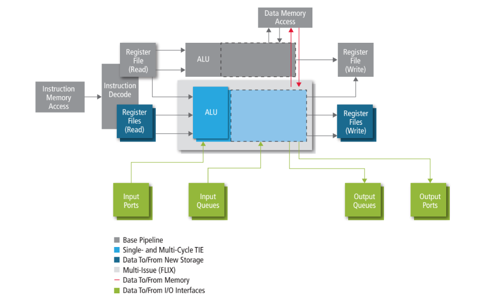
Figure 1: Xtensa processor instruction pipeline
Performance Acceleration Techniques Using TIE
TIE supports a number of techniques for performance acceleration. For details about TIE syntax or writing operations, refer to the Tensilica Instruction Extension (TIE) Language Reference Manual.
Using Fusion
Fusion increases performance by combining multiple operations into a single instruction. In programming, loops are commonly used to iteratively calculate the resulting value. For example, the following C code shows an inner-loop code of a simple C for-loop:
unsigned int a[N], b[N], c[N], i ;
for (i = 0; i < N; i++) {
c[i] = (a[i] + b[i]) / 2 ;
}
Compiling this code on the Xtensa processor results in the following disassembly code for the inner for-loop:
…
add.n a9,a11,a10
srli a9,a9,1
…
}
Notice that two instructions are executed sequentially. The first operation, add.n, calculates the two’s complement 32-bit sum. The second operation, srli, shifts the contents by a constant amount encoded in the instruction word right (inserting 0s on the left). Each iteration of the for-loop executes in two cycles.
With TIE, we can fuse the two operations into a single new operation called addshift that performs both the add and shift operations at the same time.
Now, compiling the for-loop using the new fused operation, the disassembly code shows the fusion operation addshift that executes in a single cycle:
…
addshift a12,a10,a8;
…
}
The TIE file contains the TIE code for this new operation as shown in Figure 2. For details on syntax and how to define the operation, see the Tensilica Instruction Extension (TIE) Language Reference Manual.
operation addshift {out AR avg, in AR A, in AR B} {}
{
assign avg = (A + B) >> 1 ;
}
The unique name addshift is assigned to this new operation definition. The TIE Compiler automatically generates an opcode for the addshift operation, and all Xtensa software tools are automatically updated to understand the function and timing of the addshift operation.
Note that Address Register (AR) is a predefined type that refers to the processor’s general AR register file.
The behavioral description for this operation is the combinational logic between input and output operands. By default, the operation executes in a single cycle, but you can also create multi-cycle operations (described in more detail later in this white paper). You can use expressions to compute values and assign to output operands or temporary wires. Use assign for assignment to any out or inout operand. Use wire to instantiate a local expression (more about wires later). Note that each wire, out, or inout operand can only be assigned once. In this example, the sum of input operands A and B is right-shifted once (divide by two) and assigned to the avg output operand.
Exploiting Data-Level Parallelism—SIMD Example
Single instruction, multiple data (SIMD) functionality is used to increase performance by executing the same computations on independent vector data.
For example, in the following C code, the sum is calculated for each iteration of the for-loop on independent data:
unsigned short
A[VECLEN],
B[VECLEN],
sum[VECLEN] ;
for (i = 0; i < VECLEN; i++){
sum[i] = A[i] + B[i] ;
}
The loop execution can be accelerated by performing multiple additions per cycle. A TIE register file can hold the SIMD data and create a new instruction that simultaneously performs multiple additions:
regfle simd64 64 16 v // 16-entry register fle that is 64 bits wide
operation vec4 _ add16 { out simd64 res, in simd64 A, in simd64 B } { }
{
wire [15:0] rtmp1 = A[15: 0] + B[15: 0] ;
wire [15:0] rtmp2 = A[31:16] + B[31:16] ;
wire [15:0] rtmp3 = A[47:32] + B[47:32] ;
wire [15:0] rtmp4 = A[63:48] + B[63:48] ;
assign res = { rtmp4, rtmp3, rtmp2, rtmp1 } ;
}
Each entry in the TIE register file simd64 holds 64-bit SIMD data (i.e., four 16-bit values), usually referred to as a “vector.” Vectorization is the process of packing more than one data value into a larger data type for SIMD operations.
The TIE operation vec4 _ add16 performs SIMD addition with a 4X performance increase compared to the original C code.
simd64 A[VECLEN/4]; // Input vectors
simd64 B[VECLEN/4]; // Input vectors
simd64 sum[VECLEN/4]; // Output vectors
for (i=0; i<VECLEN/4; i++){
sum[i] = vec4 _ add16(A[i],B[i]);
}
Using FLIX to Issue Multiple Operations in Parallel
TIE allows you to pack multiple operations into a single instruction that executes in a single cycle. The Xtensa processor uses an innovative approach to VLIW design called FLIX (Flexible Length Instruction eXtensions), which gives you the flexibility to modelessly intermix smaller instructions with multi-operation FLIX instructions. By packing multiple operations into 32-bit to 128-bit instructions in 8-bit (1-byte) increments, FLIX allows you to accelerate a broader class of embedded applications while eliminating the performance and code-size drawbacks of conventional VLIW processor architectures.
For example, consider code for a simple C for-loop:
for (i=0; i<n; i++)
c[i]= (a[i]+b[i])>>2;
Compiling this code on the Xtensa processor without the FLIX implementation results in the following disassembly code:
loop:
…
addi a9, a9, 4;
addi a11, a11, 4;
l32i a8, a9, 0;
l32i a10, a11, 0;
add a12, a10, a8;
srai a12, a12, 2;
addi a13, a13, 4;
s32i a12, a13, 0;
The compiler executes the for-loop code one instruction at a time without FLIX, taking eight cycles to execute a single iteration, where the total cycles is based on n iterations.
Adding FLIX to your Xtensa processor improves performance by issuing multiple operations in parallel. With some additional hardware for parallel processing, a FLIX implementation can greatly reduce the overall execution cycles of your application program.
When compiling the same for-loop code on the Xtensa processor with a 64-bit FLIX implementation, three operations can be bundled in a single instruction, resulting in the following disassembly code:
loop:
{ addi ; add ; l32i }
{ addi ; srai ; l32i }
{ addi ; nop ; s32i }
With FLIX, the compiler executes the for-loop code in three cycles, which is a tremendous performance improvement versus the eight cycles without FLIX. In this case, FLIX bundles a maximum of three operations in a single instruction word where possible for parallel processing.
Note that a NOP (no operation) operation is inserted in a slot when an operation cannot be placed for parallel execution. The compiler can choose to use FLIX or not from one instruction to the next without penalty so that it does not need to insert NOP operations each time.
Refer to the Increasing Processor Computational Performance with More Instruction Parallelism white paper for more details.
Optimizing a Function: pop_count
This example shows various methods of accelerating performance for a commonly used function.
For some algorithms, it is useful to know how many bits in a register are set to a value of 1. For example, an OS may want to know how many interrupt request bits are set, or a compression routine may need the Hamming distance of a string. The task of counting the number of 1s in an operand is called population count, or pop _ count. Many C compilers have a built-in function for pop _ count.
Various software algorithmic methods and hardware TIE implementations can be incorporated to improve the pop _ count computation performance, reducing the needed compute cycles.
For example, the following basic C routine performs pop _ count for a 32-bit value:
// unsigned int x contains input value
unsigned int y=0;
unsigned int i;
for(i = 0; i < 32; i++) {
if((x&1) == 1) y++; // Increment counter if bit is set
x = x >> 1; // Shift to prepare for next bit
}
// y contains result
This code steps through each bit of a 32-bit operand, and if that bit is 1 it increments a counter. Note that the loop always performs 32 iterations. This algorithm takes ~70 clock cycles to perform, which is an expensive implementation since throughput is low and power consumption is high.
The pop _ count computation can be optimized using various clever techniques. For example, you can reduce the 32 loop iterations down to only iterate as many times as there are 1s in the operand. Assuming an even probability distribution, on average the loop would iterate 16 times. This C algorithm translates into a binary subtraction and a logical AND operation to compute the pop _ count value.
// x contains input value
// count returns pop count
unsigned int x;
unsigned int count;
for (count=0; x!=0; count++) {
x &= x-1;
}
// count contains result
This code shows the assembly for the inner-for loop, which translates to two instructions:
// R2 contains the operand
// R1 is a temp reg
SUB R1, R2, 1
AND R2, R2, R1
Assuming 14 clocks, we now have 46 cycles on average to compute pop _ count compared with the previous 70 clock cycles, which is a 1.5X speedup compared to the original C routine. Changing the algorithm cuts time and reduces energy
With the Xtensa processor, we can define a new TIE instruction, DECR _ AND, to fuse the subtraction and logical AND operations into one new operation:
operation DECR _ AND {out AR count, in AR x}{}{
assign count = x & (x -1);
}
The assembly for the inner-for loop using the new TIE instruction is just one instruction:
// R1 contains the operand
DECR _ AND R1, R1
By adding the TIE instruction, we save 16 clocks, reducing from 46 to 30 cycles for a 2.3X speedup compared to the original C routine.
Additionally, further performance improvements can be achieved by combining different software algorithm techniques. For example, using stored constants, we can replace the loop with C statements that sum adjacent bits, bit pairs, nibbles, and bytes, while accumulating the result each time. These computations can be performed using SHIFT, AND, and ADD instructions. The disadvantage of this method is that the constants need to be preloaded into registers, incurring load operation overheads.
Alternatively, we can use an all-hardware implementation to overcome the limitations of software by directly building a pop _ count instruction in the Xtensa processor.
The new C code is:
// unsigned int x contains input value
unsignedint y = POP _ COUNT(x); // single cycle
// y contains result]
The TIE definition for the pop _ count operation is:
operation pop _ count {out AR co, in AR ci}{}{
wire [3:0] a0 = ci[0] + ci[1] + ci[2] + ci[3] + ci[4] + ci[5] + ci[6] + ci[7];
wire [3:0] a1 = ci[8]+ci[9] + ci[10] + ci[11] + ci[12] + ci[13] + ci[14] + ci[15];
wire [3:0] a2 = ci[16]+ci[17]+ci[18] + ci[19] + ci[20] + ci[21] + ci[22] + ci[23];
wire [3:0] a3 = ci[24]+ci[25]+ci[26] + ci[27] + ci[28] + ci[29] + ci[30] + ci[31];
wire [5:0] sum = a0 + a1 + a2 + a3;
assign co = {26’b0, sum};
}
TIE wires are used to create complex expressions from a set of simple expressions that can be declared, assigned, and used within a TIE operation. Each TIE wire can be assigned only once and can be used any number of times.
The entire pop _ count function can be reduced to a single operation that executes in a single cycle, providing a 70X speedup over the original basic C code. A hardware designer would take this solution, but a programmer, limited by off-the-shelf processors, has to find ways around the hardware limitations. TIE and Xtensa processors allow programmers and hardware designers to collaborate in the design space without barriers to make highly effective and efficient targeted processors.
Customizing Storage—Adding a Register or Register File
The Xtensa instruction set architecture (ISA) defines a general-purpose AR register file with access to sixteen 32-bit registers.
A specific data width can be desirable to optimize processing performance, reduce system bandwidth overheads, and save memory. For example, if an application requires a 24 x 24 multiply with a 56-bit accumulate, it is inconvenient to use a 32-bit AR register file for storing the accumulator. You would need two AR registers to hold the 56-bit value (wasting bandwidth) and more instruction encoding bits, and the number of ports on the AR register file may increase.
Xtensa processors offer two types of architectural storage:
- A single instance of a register called state
- Register files
A TIE regfle directive adds a new register file to the processor that can be up to 1,024 bits wide and have up to 128 entries. You can add multiple TIE register files to meet your application’s needs.
For a SIMD example, we can add a 64-bit, 16-entry register file called simd64:
regfle simd64 64 16 v // 16-entry register fle that is 64 bits wide with v
// as the short name
The new register file can be used in any TIE operation as an input, output, or inout operand. It can be listed in the explicit operand list, and will be visible in assembler syntax and in an intrinsic argument list. The number of read/ write ports is determined by the TIE operations that use the register file. The following example uses simd64 for various operand types:
operation add64 { out simd64 res, in simd64 A, in simd64 B } { }
{
assign res = A + B ;
}
Adding I/O Interfaces to the Xtensa Processor
Designers can add multiple I/O interfaces to the Xtensa processor to execute data transfers in a single cycle or with a fixed latency. As shown in Figure 3, multiple Ports (GPIO), Queues (FIFO), and memory Lookup interfaces can be added that bypass the Xtensa load/store units altogether. These interfaces are simple, direct communication structures. Transactions conducted over these interfaces are not accessed by addresses supplied by the processor. Instead, these simpler structures are accessed by TIE instructions that implicitly initiate the transactions. Transactions over Ports and Queues execute in a single cycle, and over Lookups with a fixed latency. One custom instruction can initiate transactions on several interfaces at the same time to boost I/O bandwidth per cycle by two or three orders of magnitude.
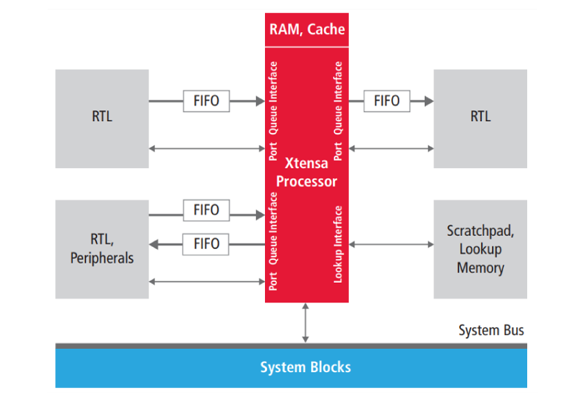
Figure 3: Ports, Queue, and Lookup interfaces allow direct data transfers
Ports
Ports act like general-purpose I/Os (GPIOs) and are wires that directly connect two Xtensa processors or an Xtensa processor to external RTL. Port connections can be up to 1,024 wires wide, allowing wide data types to be easily transferred without requiring multiple load/store operations. Ports are particularly useful to convey control and status information.
Ports do not implement any handshake mechanism to tell the external world when a value is updated on an output port or when a value is read from an input port. There are two TIE Port types:
- Export State—State made visible to the external world
- Import Wire—External wires made visible to the data path of an Xtensa processor
See the High-Speed Alternatives for Inter-Processor Communications on SOCs white paper for additional information.
Queue Interfaces
Queue interfaces enable simple connectivity from an Xtensa processor to external synchronous, first-in-firstout (FIFO) devices. Two types of Queue interfaces can be created: an input Queue interface and an output Queue interface. The Queue interface adds wide datapaths and handshake signals that allow data to move every cycle. In the simplest case, you can create TIE instructions that pop data from input Queues and push data onto output Queues.
Figure 4 shows an output Queue interface. Three ports are created for every output Queue interface (TIE _ MY _ OQ _ Full, TIE _ MY _ OQ _ PushReq, and TIE _ MY _ OQ[31:0]).
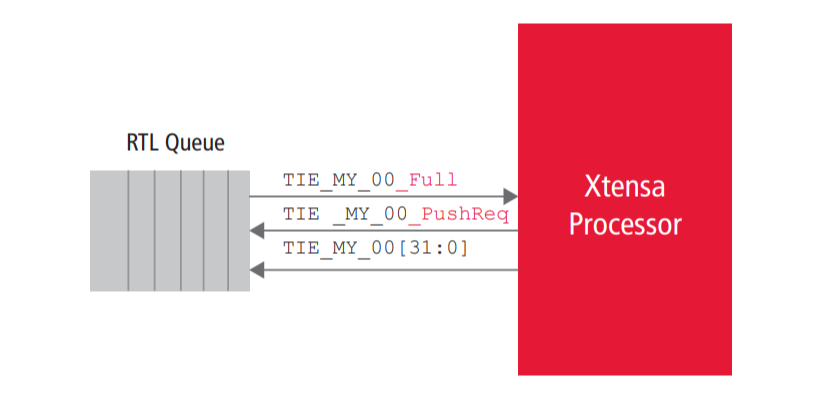
Figure 4: Example of a TIE output Queue Interface
This TIE code defines a 32-bit output Queue interface called MY _ OQ:
queue MY _ OQ 32 out
operation MY _ PushQ
{in AR qdata}
{out MY _ OQ} {
assign MY _ OQ = qdata ;
}
The pushed value can either come from an input operand or can be computed within the instruction.
Example C code using this Queue is:
#include
…
int data = 12 ;
MY _ PushQ(data) ;
…
Similarly, an input Queue interface is defined with three ports: TIE _ MY _ IQ _ Empty (input), TIE _ MY _ IQ _ PopReq (output), and TIE _ MY _ IQ[31:0] (input).
Lookup Interfaces
A Lookup interface is a useful extension for directly connecting to external memories (e.g., ROM and RAM) for performing table lookups, or connecting to special-purpose hardware with fixed latencies (e.g., other RTL). The Lookup structure designates both input and output ports so that a TIE operation can send out a value, perhaps a command or address, and receive back data within the same instruction (a specified number of clock cycles later). Note that a TIE operation can access multiple wide memories simultaneously. Lookups are not in the memory address space of the processor, so code running on the processor can get fast access to special memories or banks of external registers without slow, 32-bit wide load/store bottlenecks that must be conducted over the processor’s bus.
Lookups perform atomic transactions with an output phase where a request is made (and the Xtensa processor outputs the address) followed by an input phase where a response is expected (e.g., external logic returns the data). A Lookup can specify the delay in clock cycles between the output request and the corresponding data response. Even though a lookup is a multi-cycle access, lookup requests are fully pipelined.
See the High-Speed Alternatives for Inter-Processor Communications on SOCs white paper for more information on Ports, Queues, and Lookups.
Using TIE Intrinsics in C Programs
Intrinsic functions are widely used by compilers for performing architecture-specific optimizations from C or C++ code. For instance, Microsoft compilers use intrinsics to generate assembly containing X86 SIMD instructions. Intrinsic functions enable the use of TIE instructions in C or C++ programs.
TIE developers can define operations on user-defined TIE data types to use standard C operators (such as +, -, * and /), allowing C programmers to use a more natural programming style, without intrinsics. The syntax is similar to an in-line function. The arguments are standard C or user-defined data types. An intrinsic implementation is handled by the Xtensa C/C++ Compiler (XCC), which checks the type of input/output arguments, performs necessary data movement, and translates into TIE instructions.
A C file contains the following code:
#include <xtensa/tie/avg.h>
unsigned int a[N], b[N], c[N], i;
for (i=0; i<N; i++) {
c[i] = addshift(a[i], b[i]);
}
For the XCC compiler to understand the intrinsic, the C file must include the header file, which contains the prototype definition of the addshift intrinsic.
Similar to a C function, a TIE intrinsic can have type 32-bit signed constants, variables of C, or user-defined data type input/output arguments. Each argument can be an input, output, or inout.
The TIE intrinsic prototype definition closely resembles the C function prototype definition. It contains the forward declaration of the TIE intrinsic that omits the function body (implementation) and describes the TIE intrinsic’s return type, name, and input argument types. The prototype definition can be described in the TIE header file or ISA HTML.
Conclusion
By writing a few lines of basic TIE commands, you can easily optimize an Xtensa processor for your application. You can add new operations that reduce execution cycles, and create additional I/O interfaces that accelerate communication. The examples discussed in this white paper provide a glimpse of the power of TIE and how easily and quickly you can customize the Xtensa processor to meet your application’s needs, providing optimum results not achievable from standard processors and avoiding lengthy RTL design and verification times.
Refer to the Tensilica Instruction Extension (TIE) Language Reference Manual and the Tensilica Instruction Extension (TIE) Language User’s Guide for more details on the TIE commands and advanced features.
Additional Information
For more information on the unique abilities and features of Cadence Tensilica Xtensa processors, see IP