- Design Overview
- Distributed Simulation
- Sigrity Product Line Overview: SI/PI for PCBs and IC Packages
- Hybrid Solver and Advanced PI Updates
- Sigrity User Experience and Features: Introducing the Layout Workbench
- SI/PI Performance Improvements
- Signal Integrity Updates
- Case Studies: PowerSI, DDR5, and System-Level PI
- Conclusion
White Paper
Sigrity X - Redefining Signal and Power Integrity
This white paper highlights the features in Cadence Sigrity X signal and power integrity (SI/PI) solutions for system-level SI and PI analysis that enable designers to cut the number of design respins and meet short time-to-market windows with confidence.
Overview
Design Overview
Cadence’s next-generation Sigrity solutions are redefining SI and PI analysis with a performance increase of up to 10X while maintaining the trusted accuracy for which Sigrity tools are known.
The Sigrity X tool suite addresses the size and scalability challenges of system-level simulations faced by today’s leading-edge technologists in the 5G communications, automotive, hyperscale computing, and aerospace and defense industries. It features powerful simulation engines for system-level analysis and includes the innovative massively distributed architecture of the flagship Cadence Clarity 3D Solver.
This next-generation release works in tandem with the Clarity 3D Solver and is deeply integrated into the Cadence Allegro PCB Designer and Allegro Package Designer Plus implementation tools. This enables PCB and IC package designers to incorporate end-to-end, multi-fabric, multi-board systems (from transmitter to receiver or power source to power sink) for SI/ PI signoff success.
Sigrity X also provides a user experience that streamlines setup time for detailed system-level SI/PI analysis by transitioning seamlessly across different analysis workflows.
Distributed Simulation
SI and PI engineers rarely have enough time to simulate an entire design and often need to take shortcuts. Selecting perceived worst-case signals to simulate as representative of large signal groups is one shortcut example; however, this approach has been known to miss critical crosstalk or simultaneous switching noise problems. Fortunately, Sigrity X now enables analysis of the full group of signals in a short timeframe. The combination of rearchitected engines that efficiently utilize the cores on a single machine plus the ability to distribute the simulation to two or more computers allows the large group of signals to simulate in a similar time frame as the shortcut “worst-case” signal simulation. The additional simulation coverage gives SI/PI engineers greater confidence that designs will be ready on time for manufacturing a prototype.
This concept of distributed simulation is in the DNA of Cadence multiphysics analysis tools. The Voltus IC Power Integrity Solution massively distributes its PI solution for ICs across multiple computers. The Clarity 3D Solver has taken full-wave 3D analysis to the next level. The Celsius Thermal Solver also distributes thermal technology across multiple computers, and the Clarity 3D Transient Solver addresses electromagnetic interference (EMI) analysis simulations across multiple computers. And now in Sigrity X, designers are seeing distributed computing and multiphysics in new ways that enable them to address SI and PI problems much faster and iterate much more quickly than ever before, with the same trusted accuracy.
Figure 1 showcases endorsements from the best-known names in the industry, which were included in the announcement of the product. These endorsements testify that the 10X faster simulation time has cut weeks off design cycles, turnaround time has gone from days to hours, projects are finishing weeks earlier with the same accuracy, and quality has increased through the ability to run more thorough simulations quickly enough to meet schedules.
“Our continued success in the 5G mobile, home entertainment, networking, and other industries depends on design and analysis tools that keep up with thriving markets and demanding time-to-market schedules. We work closely with the Sigrity team from Cadence and are very pleased to see the results being delivered in the next-generation Sigrity release. Not only can many designs be analyzed 10X faster with the same accuracy level, but the capability has also been extended to larger and more complex designs that previously could not be analyzed. This productivity builder is allowing us to cut weeks off our design cycles and expedite our product delivery.”
Aaron Yang, Senior Director at MediaTek
“We depend on fast and accurate modeling tools for the advanced IC packages we design for our foundry customers. Using the tightly integrated Allegro Package Designer Plus and Sigrity XtractIM tool combination from Cadence has been key to our many successes. The Sigrity 2021 release brings us the same level of accuracy from the Sigrity XtractIM field solver with performance that can allow us to deliver final design plans weeks earlier than before. Along with another 10X performance improvement from Cadence, we are looking forward to delivering a better product to our customers.”
Sangyun Kim, VP of Foundry Design Technology at Samsung Electronics
“In a world with increasing speed and scale, there is a growing need to verify systems accurately and quickly in order to deliver Renesas products to the data center, industrial, and automotive markets in a timely manner. Using the new Sigrity 2021 release, important processes for IC package signoff were improved dramatically; simulations that took more than more than a day to complete can now be completed in just a few short hours. We are excited about the adoption of this new technology, with a proven performance improvement of 10X, for our production designs.”
Tamio Nagano, Senior Principal Engineer, Design Automation Department, Shared R&D EDA Division, IoT and Infrastructure Business Unit at Renesas
“Our high-speed interfaces such as 56G SerDes and LPDDR5 must meet strict integrity requirements. Our design teams require that our PCB design and analysis tools work seamlessly. The combination of Cadence Allegro PCB design tools and Sigrity analysis tools gives us this seamless integration. We are now seeing ‘the X-factor’ with Sigrity technology. Sigrity X technology delivers up to 10X performance improvements over previous releases, significantly reducing the time required to analyze the PCB. We can now increase quality by iterating two or three more times and still meet our schedules. This ensures we have a robust product for our customers.”
David Dal, VP of H3C Semiconductor Technologies Co., LTD.
Figure 1: Sigrity X customer testimonials
Sigrity Product Line Overview: SI/PI for PCBs and IC Packages
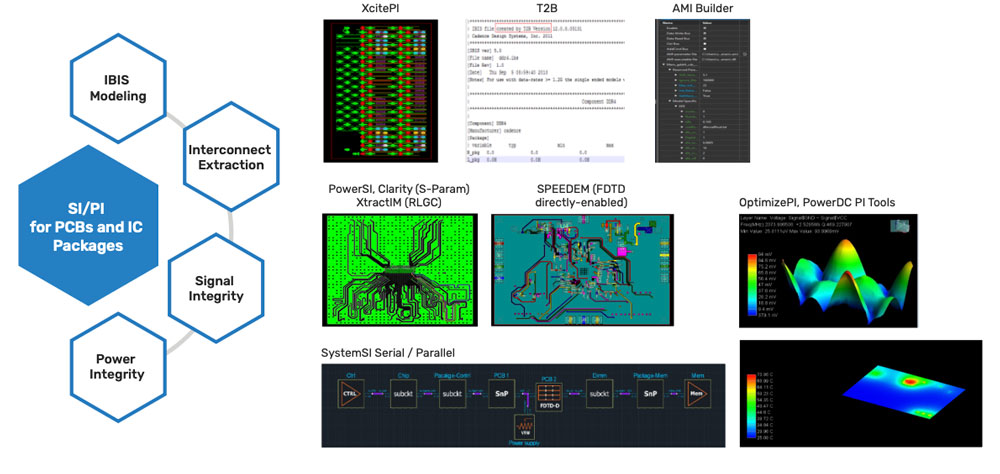
Figure 2 provides an overview of the Sigrity product line. Starting with modeling the inputs/outputs (I/Os), Cadence offers the Sigrity Advanced IBIS Modeling solution, which includes I/O buffer information specification (IBIS) modeling tools, Transistor-to-Behavioral Model Conversion (T2B) for full bus simulations, and AMI Builder technology, which models dynamic equalization. For interconnect extraction that enables solving for different substrates, Cadence has Sigrity XcitePI Extraction silicon redistribution layer and/or interposer extraction and Sigrity PowerSI EM field solver and Sigrity XtractIM technologies, which offer a hybrid solver being used for organic materials. The Clarity 3D Solver can be used for both higher fidelity high- frequency extraction and also for producing S-parameters. For SI, Cadence has Sigrity SystemSI technology for serial/parallel link analysis and SPEEDEM technology for finite difference time-domain (FDTD) analysis. Cadence power integrity tools Sigrity OptimizePI and Sigrity PowerDC optimize performance and cost and ensure reliable power delivery, respectively.
Hybrid Solver and Advanced PI Updates
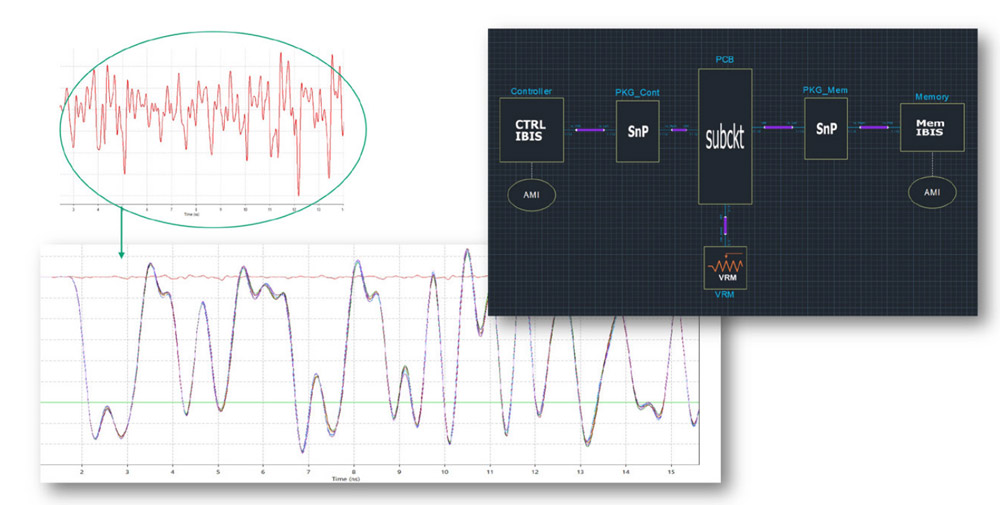
Sigrity technology is well-known for power-aware SI analysis, which utilizes both extraction and SystemSI technology for parallel bus analysis to enable power-aware high-accuracy SI analysis. In the Sigrity X release, Cadence addresses solutions for leading-edge DDR5 and 112G interfaces. The combination of gold-standard interconnect modeling along with time-domain simulation (circuit and channel simulation) for serializer/deserializer (SerDes) analysis with IBIS AMI support uniquely positions Cadence as a one-stop shop for extraction and interface compliance signoff (Figure 3).
Sigrity User Experience and Features: Introducing the Layout Workbench
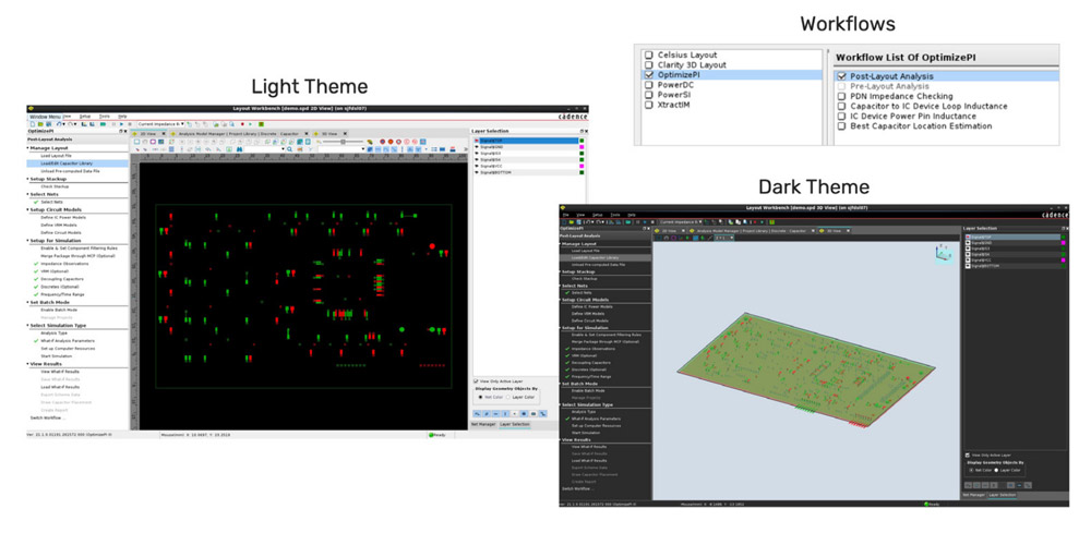
The Sigrity user interface has been updated significantly in Sigrity X, and the tools discussed in this white paper have been updated to provide a common, consistent user experience (Figure 4).
These tools natively support Microsoft Windows and Linux operating systems. Along with the infrastructure, there is a better user experience with faster interfaces and less lag time. Overall, the usability of the interface has been improved significantly. As can be seen in Figure 5, designers can choose a light or dark theme and many of the panels can be configured interchangeably. The workflows have all been migrated into the same environment, enabling engineers to switch between workflows from within the same interface.
One of the small, simple features that has drawn much interest and seems to be saving a lot of time is the ability to maximize the workspace as well as return back to the factory reset of all the panes. In addition, the menus are context sensitive, so if the user is in a specific workflow, for instance, layout editing mode, all the menu items/icons are available within that sub-window rather than having to go back to the top level.
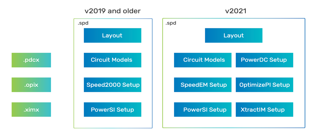
Figure 5 reflects a major change in Sigrity X—the database. In the past many files controlled the simulation, and the approach used was not consistent between various Sigrity tools. In 2021, all the data migrated into a single .spd file for all simulation types, making it much easier to copy or move simulation files between machines and also to support multiple simulation types within the same file. A second important point is that all of the Sigrity X solvers have been significantly sped up.
SI/PI Performance Improvements
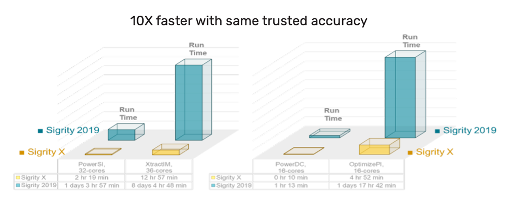
Figure 6 provides examples of improvements in Sigrity X. Because of high signaling speeds, many SI engineers now want a single interconnect model for package and PCB. The combined extraction not only provides greater accuracy than two cascaded models, but also adds the benefit of simulating interaction between signals on the package and the PCB. The PowerSI example is a package plus PCB simulation done with PowerSI tool. This formerly took almost 28 hours to simulate and now takes less than two hours and 20 minutes—a 12X improvement. This drastic improvement is an example of how what may have previously only been thought of as a signoff simulation can now be moved upstream in the design cycle giving design teams opportunities to optimize the PCB/package interface.
The XtractIM example is an integrated fan-out (InFO) package simulated using 36 cores. Due to the complexity of some of the current packages, the XtractIM tool can take much longer, in this case over eight days. With the 2021 version, the simulation took less than half a day, a performance improvement of 15.1X.
The PowerDC example is a flip-chip ball grid array (FC-BGA) package simulation analyzed with the PowerDC tool using 16 cores. Similarly, in the PowerDC tool, which is already known as a very fast solver, simulations that formerly ran over an hour now take 10 minutes—an improvement of 7.18X.
Finally, the OptimizePI simulation shows a PCB plus package simulated using 16 cores and took almost 42 hours using Sigrity 2019. With Sigrity X, the simulation took less than five hours—an 8.56X improvement.
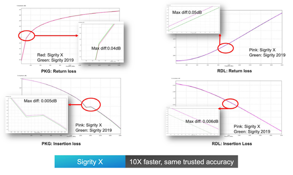
Most importantly, there is no compromise in accuracy. The re-architecture of the Sigrity engines is a step and repeat of what has been previously accomplished by the Voltus IC Power Integrity Solution, Clarity 3D Solver, and Celsius Thermal Solver where there is no loss in accuracy even though the solver is being distributed across multiple machines. Below we compare the results from the previous Sigrity release to Sigrity X. The results are virtually identical even though the simulation time is drastically reduced. (Figure 7).
Table 1 summarizes Sigrity PowerSI, PowerDC, XtractIM, and OptimizePI examples of dramatically increased simulation speeds delivered through distributed computing, code refactoring, algorithms, and multi-threading computing, all without compromising accuracy. Sigrity tools are showing faster simulations when the number of cores remains consistent, but also a nearly linear speedup when more cores are added. There is no limit to the number of computers that can be accessed at the same time when on the Linux platform.
Table 1: Sigrity tools deliver 10X faster simulations with the same trusted accuracy
| Sigrity Solver | Design Type | 2019 | 2021 Sigrity X | Speedup |
|---|---|---|---|---|
| PowerSI | PKG + PCB | 1day:3hr:57min (32 cores) | 2hr:19min (32 cores) | 12X |
| PowerDC | FC-BGA PKG | 1hr:13min:1sec (16 cores) | 10min:10sec (16 cores) | 7.18X |
| XtractIM | InFO | 8days:4hr:47min:57sec (36 cores) | 12hr:57min:25sec (36 cores) | 15.1X |
| OptimizePI | PCB + PKG | 41hr:42min:4sec (16 cores) | 4hr:52min:12sec (16 cores) | 8.56X |
| Sigrity X Scalability | 8 cores | 16 cores | 32 cores | |
|---|---|---|---|---|
| PKG | 7 hrs | 4.75 hrs | 3.4 hrs |
| Sigrity X Scalability | 8 cores | 16 cores | 32 cores | |
|---|---|---|---|---|
| RDL | 7.83 hrs | 4.87 hrs | 3.67 hrs |
The high-power computing (HPC) interface for Sigrity X should be familiar to those who already use Clarity 3D Solver. Users can either choose a local machine or distributed the job across a server farm. The simulation can access multiple computers utilizing as many cores as are available. Sigrity X supports multiple licensing techniques for increasing the simulation core count including license stacking and/or use of HPC accelerator licenses.
Signal Integrity Updates
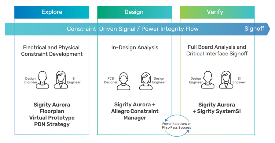
Signal integrity starts with the Cadence constraint-driven SI/PI design flow. The Sigrity engines are used directly in the Allegro canvas to provide traditional SI and PI analysis in Sigrity Aurora (Figure 8). In-design analysis (IDA) enables PCB design teams to reduce design iterations.
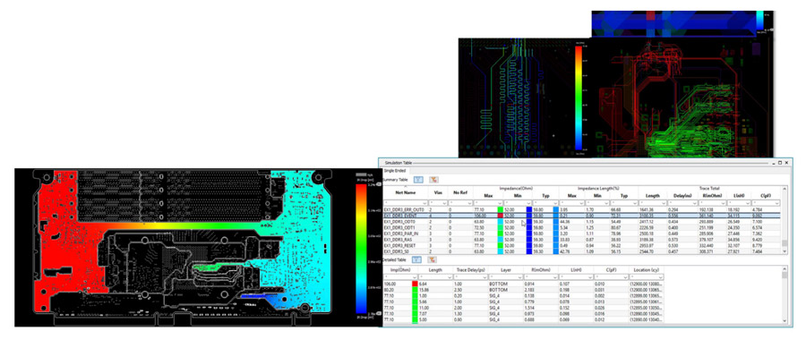
Within the Allegro design canvas, Sigrity Aurora provides access to easy-to-use workflows for prototyping, topological extractions, crosstalk and reflection analysis, IR drop, impedance, coupling, and return path simulations, all while being powered by the Sigrity X engines without leaving the design environment. This unique environment blends the best of Allegro and Sigrity technologies within the Allegro canvas (Figure 9).
Users can screen PCB designs in novel ways and streamline the design process by catching issues early in the design cycle and being able to natively edit the design without switching tools. The supplied workflow guides users with step-by-step setups and execution. By following the provided workflows, frequent users don’t need to learn a new skill or use model. Sigrity Aurora brings design engineers useful feedback in making critical design decisions.
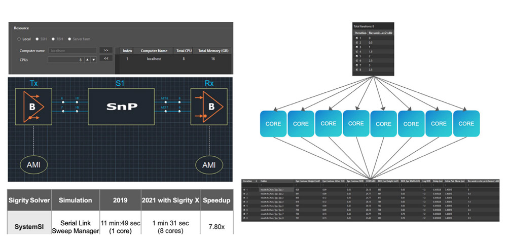
Sigrity X now provides SI engineers access to distributed computing, as shown in Figure 10.
This added capability enables designers to distribute parallel simulation jobs that allows, in some cases, almost linear speedup in simulation time. As an example, the sweep manager tool in the Sigrity SystemSI flow allows simulations to be run on a sweep of multiple parameters like algorithmic modeling interface (AMI) parameters and model parameters in the analysis options. In the past, these simulations would be run serially, and, in some cases, could take days to run. With the HPC enhancement in Sigrity X, these simulation jobs can now be run in parallel, giving designers a huge increase in productivity. In the test case shown in Figure 10, using eight cores provided an almost a linear speedup of 8X in simulation time.
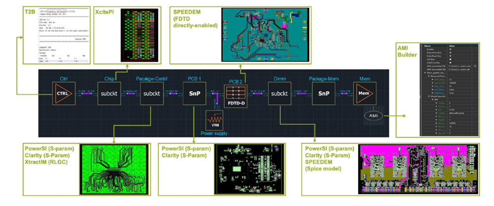
When it comes to building system-level simulations, whether it is a parallel bus or a PI analysis, Sigrity X technology covers everything (Figure 11).
For IBIS model generation, the Sigrity Transistor-to-Behavioral (T2B) Model Conversion converts transistor models to behavioral models that enable accurate and efficient serial and full bus simulations in hours instead of days. With model generation supported by up to IBIS 6.1 formats as well as the accuracy-enhanced Sigrity behavioral model format, T2B meets the needs for accurate system-level simulation that have become essential due to the rapid advancement of high-speed interface technologies.
AMI model creation has never been easier than with the AMI Builder. The wizard-based approach walks the user through a series of questions to build a block-based topology of equalizing elements. AMI Builder is used by the Cadence intellectual property (IP) group to generate the IBIS AMI models for their DDR and SerDes IP offerings, which also includes the latest edition of backchannel modeling in the IBIS 7.0 standard.
With the XcitePI tool, the user can generate models of the die redistribution layer (RDL) interconnects between the I/O cells and connections to a package. These models take into account parasitic resistance, capacitance, and inductance coupling amongst all conductors in the entire die’s power grid. It is also used for die-to-die interconnect modeling on silicon interposers.
For building accurate package and board models, Sigrity X offers multiple solutions starting with the XtractIM tool, which can help create RLGC device package electrical models using the hybrid electromagnetic (EM) solver. To perform more detailed model extractions, the PowerSI tool can provide fast, accurate, and detailed models of full IC packages, PCBs, or merged PCB and IC packages via a hybrid solver analysis engine. And for the most detailed model generation, Clarity distributed multiprocessing technology enables the Clarity 3D Solver to generate full-wave S-parameter models with unmatched speed and capacity.
SPEEDEM technology integrates with the SystemSI simulation to provide another way of modeling a wide parallel bus. SI engineers can use the FDTD-direct method without having to create an S-parameter. This technology enables power-aware SI analysis of a memory bus without having to extract a large, 100-port S-parameter.
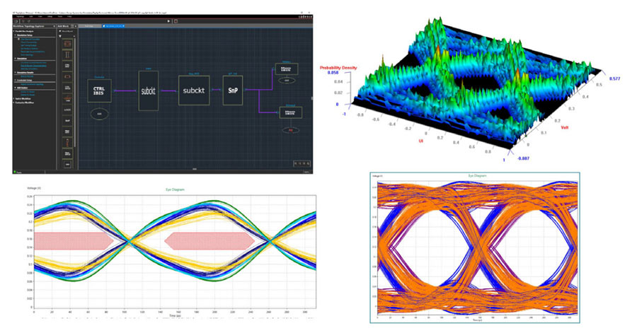
Sigrity X provides a complete set of tools for doing the latest double data-rate 5 (DDR5) simulation and enhanced data-dependent measurements (Figure 12).
With AMI Builder, building DDR5 models with the now-required decision feedback equalization (DFE) for the controllers and continuous time-linear equalization (CTLE) and DFE for the memory is easily done. For signoff, a custom report generator ensures all the needed checks are meeting specification.
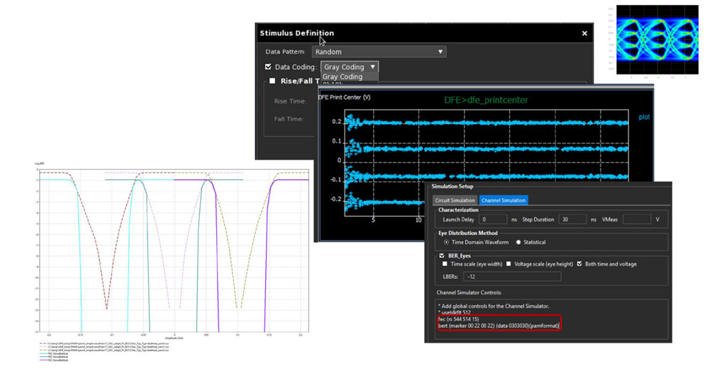
With ever-increasing demand for higher throughput in serial links, Sigrity X is able to handle the latest PAM4 analysis requirements (Figure 13). This includes gray encoding and decoding of the simulated data pattern, RX center eye plots for deeper post-simulation analysis, the application of the popular Reed-Solomon forward error correcting (FEC) algorithm to assess the improvement of bit-error rate (BER), and a virtual BER tester (BERT) functionality for bit-error rate analysis.
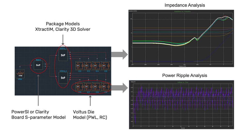
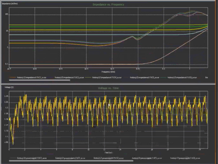
Lastly, a tool is now available for performing system-level power domain analysis (Figure 14). With board and package power delivery network (PDN) models created using Sigrity PowerSI technology, Clarity 3D Solver, and die models created by the Voltus IC Power Integrity Solution, designers can now perform multi-fabric and/or multi-board power-domain analysis in just one tool, impedance analysis of the entire PDN, IR drop analysis, and power ripple analysis to ensure all PDN requirements are being met. IC design teams can also use this tool to create target impedance curves that can be provided to their systems customers.
Case Studies: PowerSI, DDR5, and System-Level PI
Example 1: Setting Up a Sigrity X Simulation
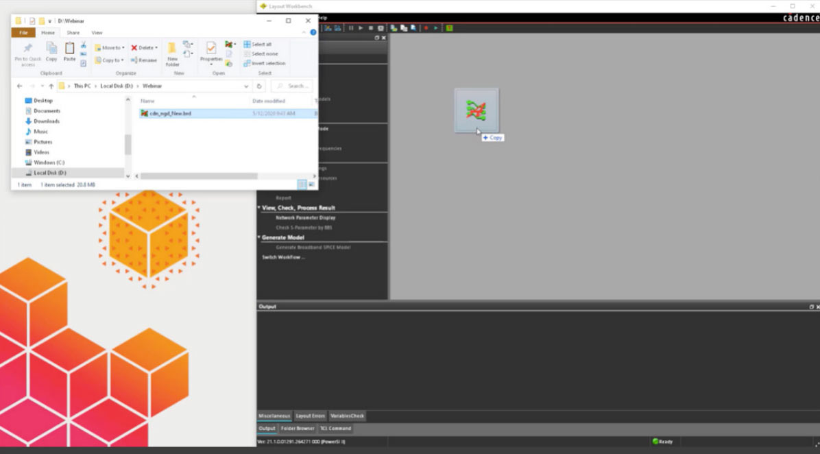
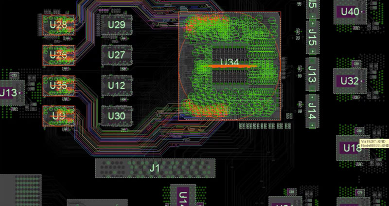
Figure 15 shows the Sigrity user interface in the dark theme. The example starts by dragging and dropping the .brd file into the window.
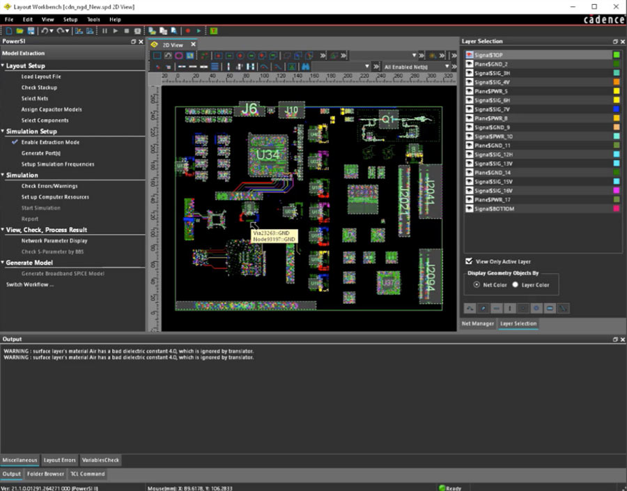
The file is quickly translated (Figure 16) to the layout window.
The few quick and easy steps necessary to go from layout all the way to results follow.
Step 1: Select Load Layout File from the workflow pane on the left side to load the existing design database in SPD format
Step 2: Select Nets from the workflow pane to choose the nets you wish to simulate
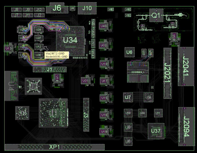
Figure 17 shows the DDR interface fully selected. The ports of interest are at the top left.
Step 3: Select Assign Capacitor Models from the workflow pane to assign SPICE or Touchstone models. The SPICE models are not limit to RLC definitions—any passive network in any combination can be used.
Step 4: In Simulation Setup, Enable Extraction Mode is already selected, so the next step is to generate ports based on enabled nets.
Step 5: Under Simulation the computer resources can be set up. In this example, there are eight cores and 32Gb of memory on a local host. If this simulation was being run on a Linux server or farm, a distributed solve could be performed.
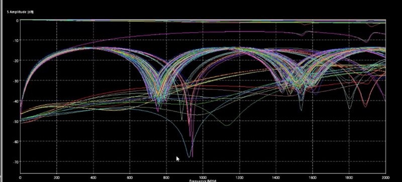
Figure 19 shows the simulation results.
Example 2: DDR Testbench
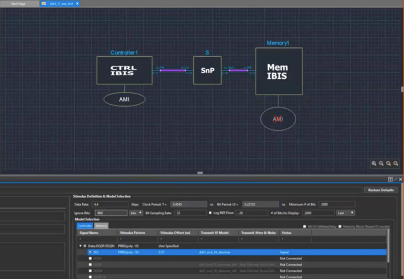
The results of the simulation in Example 1 are now put into a simple DDR test bench and a simulation run on a single DQ line (Figure 20).
The steps for Example 2 are as follows.
Step 1: Under Analysis Options choose Circuit Simulation and choose the SPDSIM simulator, or if running Linux, Spectre simulation is always an option.
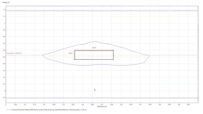
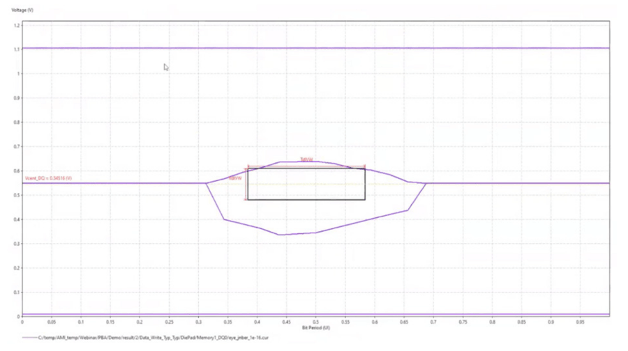
Figure 21 shows the simulation results. The left window shows the time-domain results and the right window shows the 3D results.
Step 2: Generate the channel report for the simulation by clicking on Generate Report and select the waveform location and measurement range, as well as several different thresholds. Other options include the DQ/CA mask, BER, and delay.
Step 3: To see if the design can support a faster data rate, go back and set the data rate to 6.4Gbps to see how much bandwidth there is on this particular circuit.
Example 3: Power Demand Analysis
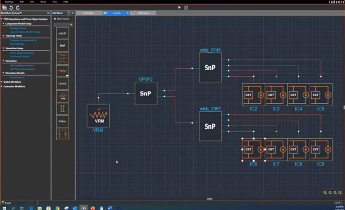
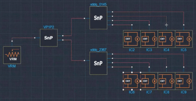
This example presents a flow for power domain analysis, shown in Figure 25.
There are various building blocks, including subcircuits, S-parameter blocks, ideal elements, layout elements, VRMs, Voltus blocks, and an IC block.
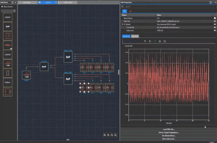
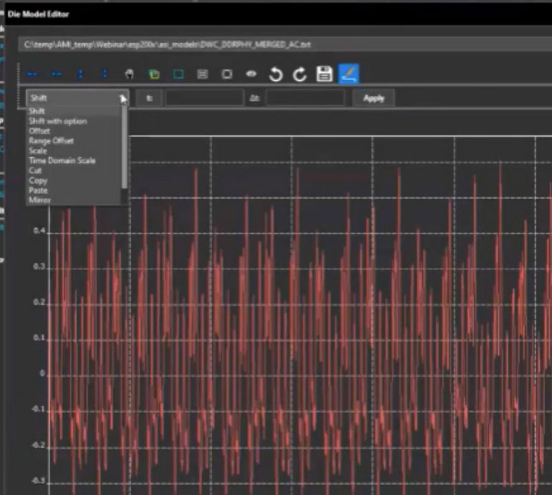
Step 1: Begin with the IC block to describe what the on-die power demand looks like.
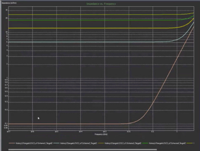
Step 2: Once the IC model is defined, the target impedance needs to be generated. In the background various other Sigrity tools are being used to provide various target impedances that can be fed back to the board package designers. After the simulation is completed on the target impedance, Figure 28 shows the results. This reflects the multiple solutions that will meet the given power ripple spec, along with the PWL of the IC.
Once these currents are generated, they can be fed back to the design team to have the targets met. Once layouts are generated from the package and board designers, a complete flow can be put together to be able to look at impedance analysis and power ripple analysis.
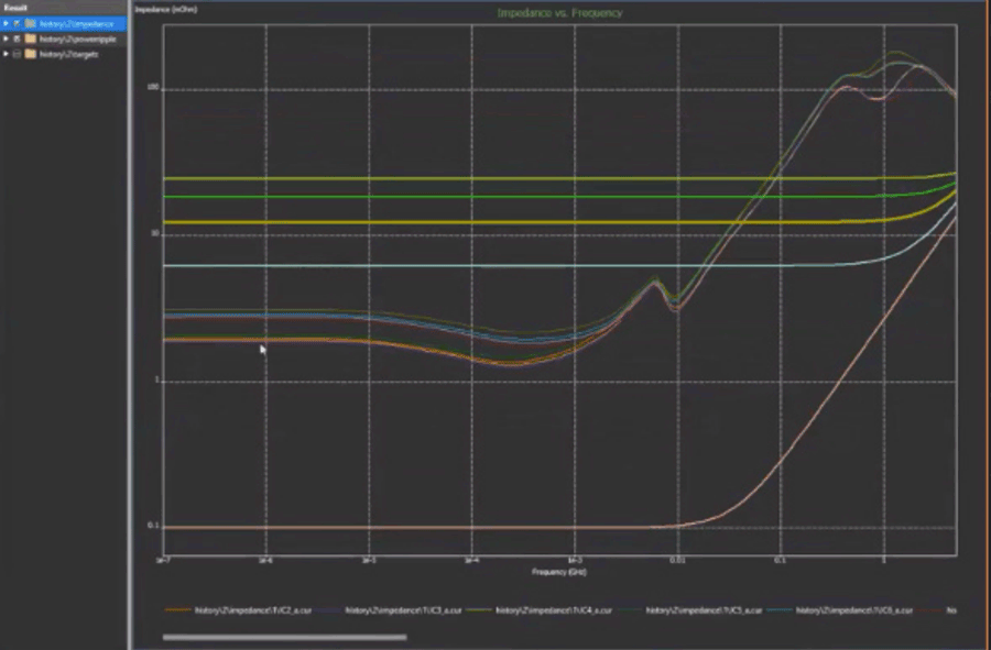
Step 3: Now that the designer has the setup, the impedances on all eight of the nodes can be examined and compared to the existing target impedances. Figure 29 shows an overlay of all eight of the target impedances of the ports. It can be seen that for some of the lower frequencies most of the target impedances are being met, but some are definitely peaking out at above about 100MHz. This might be an indication back to the design team that some of the impedance above 100MHz might need to be reduced as it may not be meeting the power ripple specification.
With this tool, a system-level power analysis can be pieced together to examine in-depth both the impedance and power ripple results.
Conclusion
Sigrity X and the Clarity 3D Solver have created a sea change in SI/PI analysis. The powerful 2021 Sigrity simulation engines for system-level analysis and innovative distributed architecture of the flagship Clarity 3D Solver have delivered tools and techniques to raise the confidence level of design teams before manufacturing a prototype. The Sigrity X user experience that streamlines setup time for detailed system-level SI/PI analysis by transitioning seamlessly across different analysis workflows has also been demonstrated through three examples highlighting an SI simulation setup, a DDR testbench, and a power demand analysis.
