White Paper
Revolution by Evolution: Getting to the Next Technology Breakthrough in Analog Simulation
Recent technology developments, advanced-node adoptions, and More than Moore designs have forced analog and custom IC designers to adopt new design practices that benefit from these advancements. These changes have resulted in the need to simulate larger designs with more post-layout parasitics. In addition, many custom IC designs such as flash memory, MRAM, sensor arrays, etc., now require SPICE-accurate simulations. To meet these demands, a new SPICE engine with much more performance and capacity than the current generation of circuit simulators is needed. The Cadence Spectre X Simulator, the next generation of the Spectre circuit simulator, has been developed to address the need for simulating the next generation of analog, mixed-signal, and custom IC designs.
Overview
Introduction
A few years back, I helped a customer with a 10-bit pipeline ADC design that had been designed by the Cadence IP Group in the late 90s. When it was built, the top-level simulation to measure signal noise and distortion (SINAD) required roughly 128 hours to complete. Running the same simulation in 2015 required about 10 minutes to run on a single CPU. Certainly, improvements in the computer hardware contributed to the simulation time improvement and about half of the improvement was due to better performing computer hardware. However, the other half of the improvement was due to advancements in the Cadence Spectre Accelerated Parallel Simulator (APS). The numerical engines in the Spectre Accelerated Parallel Simulator had been enhanced to reduce simulation time and increase simulator capacity. The practical effect of using the Spectre Accelerated Parallel Simulator along with multi-core servers was that we were able to perform design verification that was not possible in the past. For example, running a 256-iteration Monte Carlo simulation of the ADC—running the simulations on a 16-core machine— means that the simulation would be complete in under three hours.
With this, one might think that all simulation problems are solved; but the story is, of course, more complicated. The same law that benefits us causes us headaches, too—that is, while Moore’s Law [1] gives us significant boosts to simulation performance and capacity, it also presents challenges that make designers’ lives more “exciting”.
We will explore how Moore’s Law affects analog designers by considering what Moore’s Law hath wrought. Three effects of Moore’s Law on circuit simulation that need to be considered are:
-
 The effect on the design
 - The effect of process scaling
- The effect of More than Moore
Each of these factors affect designers because they increase the overall technical design challenges exponentially. Increasing their dependence on an analog simulator requires the simulator to perform better even with significant increases in circuit size and analysis challenges.
Emerging Simulation Challenges
One of the most important impacts of SoC design is that analog designers must design high-performance analog IP using the same processes that digital designers use. So, analog designs must now be designed without access to the precision transistors and passive elements that analog designers have relied on when designing in the past. As a result, designers must re-architect their circuits to take advantage of the features of deep submicron and advanced-node processes—namely, high-density logic— to implement analog functions.
New architectures
However, these new architectures place divergent requirements on simulators. On one hand, the only method to analyze linearity and noise in the time domain is to use transient analysis and then use Fourier analysis to convert the time domain response into the frequency domain response. This type of analysis may vary from analyzing offset voltages in comparators, to calibrating voltage-controlled oscillators in PLLs, determining loop-filter frequencies [3, 4], or even designing all digital PLLs [5, 6]. On the other hand, there is a need for analog functional verification because these new architectures consist of many elements that must interact correctly in many different modes of operation. Circuit simulators are required to have increased flexibility to provide designers easy options to perform many different types of simulations.
Post-layout challenges in advanced-node designs
The second effect of Moore’s Law is the effect of process scaling on circuit design. As feature size has scaled down, the relative impact of the interconnect and device parasitics has increased. Traditionally, analog designers performed most of their design testing using pre-layout schematic simulation to analyze the effect of transistors on circuit performance. The recent trend has been that even the pre-layout simulations for advanced-node designs behave like post-layout simulations due to the large number of device parasitics included in the transistor models.
The challenge of designing high-performance analog circuits with advanced-node transistors is compounded by the need to perform these simulations with parasitics since the ratio of transistors to parasitic RC elements can exceed 1:100 [7]. SerDes are particularly challenging because even if an SoC does not include analog blocks like data converters, it will still need a SerDes to serve as the I/O blocks for a digital SoC. SerDes use PLL circuits for clock generation mixed with clock/data recovery circuits. As a result, SerDes face multiple design challenges. They must be designed with advanced-node transistors that contribute a huge number of parasitic elements [8] that must be analyzed. In addition, post-layout simulation is especially important for SerDes designs because it is critical to maintain the signal integrity of the clock signal. Any noise coupling into the clock lines due to parasitics results in unwanted signal jitter in the SerDes.
More than Moore
The third effect of Moore’s Law is the effect of More than Moore, which manifests itself in bigger, highly integrated designs that can require new architectures. With this effect, increased levels of integration are not achieved with increased scaling. Alternative methods are used to increase the level of integration in advanced packaging, stacking, and new materials. For example, consider new technologies, such as 3D Flash memory and magnetic memories. 3D Flash memories can store multiple bits of data in a single memory cell [9, 10, 11, 12]. Storing multiple bits in a memory cell requires sophisticated programming and read algorithms that can only be simulated using SPICE. Magnetoresistive memories are a class of non-volatile memories that store information in magnetic domains. Unlike traditional non-volatile memories, these memory cells are programmed using current instead of voltage. This difference may seem to be small, but it has a significant impact on how the design is simulated [13]. Accurate simulation of currents requires SPICE simulations. The result is that SPICE simulations need to be scaled up to perform MRAM analysis.
Dennard’s Law
While Moore’s Law gets most of the press, there is another “law” that is affecting analog design, Dennard’s Law. Robert Dennard stated that “...with Dennard’s scaling rules, the total chip power for a given area size stayed the same from process generation to process generation.” [14] Unlike digital circuits, the power consumption of analog circuits does not scale with process technology. Reducing the power consumption of analog circuits requires developing new circuit architectures and more sophisticated power management techniques. Unlike digital designers with automated tools for power management such as unified power format (UPF) [15], analog designers must verify their designs using transistor-level simulations. Capabilities like dynamic checks have evolved to help designers identify circuit issues that can occur due to low-power design. For example, the floating gates of circuits-in during power-down cause leakage currents. However, to use checks, the circuit still must be simulated with SPICE. Not only does each mode of circuit operation need to be verified, but it also requires proper operation when switching between modes. This requires fast, but also analog-accurate verification of circuit functionality which is not possible with FastSPICE simulation.
Introducing Cadence Spectre X Simulator
The Cadence Spectre X Simulator, a massively parallel circuit simulator, provides up to 10X performance gains, while maintaining the golden accuracy customers have come to expect from more than 25 years of Spectre industry leadership. The new Spectre X Simulator can solve 5X larger designs when compared to previous Cadence simulation solutions, enabling customers to effectively simulate circuits containing millions of transistors and billions of parasitics in a post-layout verification flow. The benefits to users include proven accuracy, massively distributed simulation, faster runtime, and easy adoption, along with mixed-signal and RF solution support.
Using Spectre X Simulator for Analog and Custom IC Design and Verification
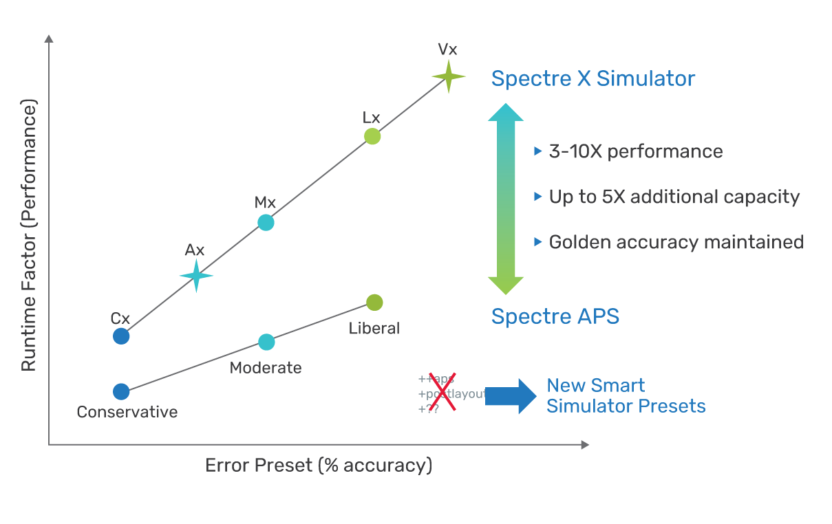
The Spectre Circuit Simulator was developed to address the accuracy concerns of analog designers and has been the trusted and golden reference for analog design for more than 25 years. The Spectre X Simulator inherits the golden accuracy of the Spectre Circuit Simulator that designers have come to expect and depend on [16]. The Spectre Circuit Simulator provided three error presets:
- Liberal, for power management other analog designs with relaxed accuracy requirements
- Moderate, for most analog applications
- Conservative, for high-precision analog applications; for example, 16-bit ADC dynamic range simulations
These error presets have served analog designers well, allowing them to tune in the accuracy they need without having to tune the simulator options. However, as we have discussed the types of simulations designers need to perform has increased and as a result the Spectre X Simulator has provided new error presets. Since the Spectre Circuit Simulator was originally developed, simulation technology has advanced, and with the introduction of the Spectre X Simulator, the error presets have been refreshed. Five error presets, cx, ax, mx, lx, and vx, provide more granularity in control of simulator along with significant boosts in performance all while maintaining the Spectre Simulator golden accuracy. The error presets are:
- vx, for custom IC verification
- lx, for power management and other relaxed analog applications
- mx, for most analog applications
- ax, for high-precision analog applications
- cx, when a golden reference is required
However, just reducing simulation time is not enough; as we have discussed, the designs are becoming larger and larger with more parasitics, more modes to simulate, and more simulations to run. The Spectre X Simulator has been enhanced to increase the capacity of the matrix solver, and the capacity has been increased by 5X as compared to the Spectre Accelerated Parallel Simulator. As a result, the Spectre X Simulator can simulate designs of more than 20 million transistors and one billion parasitic devices without sacrificing accuracy.
In addition to the enhancements to the core simulation technology, the Spectre X Simulator has a built-in smart simulation approach to the design tasks. Smart simulation is the capability of the simulator to intelligently optimize and adapt to the design, enabling technologies for post-layout simulation or high-voltage simulation, etc., as required, based on the design to be simulated. The impact of all these enhancements is improved verification for a wide variety of designs. See Figure 2.
Massively Distributed Simulation
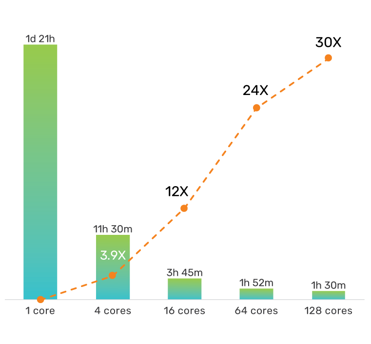
The Spectre X Simulator leverages modern compute hardware to perform scalable, massively distributed simulation. Its Xscale technology enables efficient distribution of transient and harmonic balance (HB) simulations. The Xscale technology has been tested on networks using up to 128 cores at a time on different machines, enabling massively parallel runs and expanding today’s circuit limits by up to 5X. Before distributing the simulation jobs, the simulation circuit matrix must be broken up into parts and solved on different devices. Several challenges have been overcome to make sure that breaking up the simulation into parts does not degrade the accuracy of the simulation results.
- Balancing the load between the multiple processors involved: Load balancing mitigates the bottlenecks of the simulator running on a single processor, which slows down the entire simulation.
- Optimizing communications between processors: SPICE simulation uses a single-time step and the coupling between the different pieces of the circuit matrix distributed across the hardware means that information needs to be shared at each time step.
A CMOS image sensor is an example of a design that benefits from the distributed simulation. A CMOS image sensor consists of an array of pixels; each column of pixels is connected to a sensor consisting of a signal processor including an ADC. If the transfer function of each signal processor is not matched to the transfer function of every other column, then there will be artifacts in the image, for example, the blue of the sky in the background of a picture will change color.
Differences in the transfer function result from voltage drops in the power-supply mesh. So, analysis of a CMOS image sensor is the perfect storm for SPICE simulators: very high accuracy requirements in timing and voltage, the designs are physically large, and the simulations need to include the layout parasitics. This combination has made verification of CMOS image sensors into a previously unsolved challenge. Shown in Figure 3 is the performance speed-up from distributed simulation for a CMOS image sensor when using the Spectre X Simulator. The 30X speed-up in simulation time reduced it from one-anda-half days to one-and-a-half hours.
Ease of Adoption
The Spectre X Simulator is a new addition to the Spectre Simulation Platform. Because the Spectre X Simulator is built on the Spectre Simulation Platform, it inherits the Spectre infrastructure functionality. For example, reading Spectre netlists and supporting the same models, the same stimulus, etc., enables drop-in replacement for the Spectre Accelerated Parallel Simulator, allowing all existing designs and testbenches to take advantage of the increased performance and capacity that the Spectre X Simulator provides without any changes or editing required. With the introduction of the Spectre X Simulator, additional error presets have been introduced, which are powerful modes for designers to select the appropriate simulation runtime and accuracy based on their design requirements without having to tune the simulator. In the discussion of the effect of Moore’s Law and Dennard’s Law, there is a need for the Spectre X Simulator to address new applications: memories and functional verification of low-power application, resulting in the need to provide additional error presets. The Spectre X Simulator can also be used as the analog solver in the Spectre AMS Designer simulator, enabling verification of large mixed-signal designs, and used with the Spectre RF Option, to accelerate HB analysis.
Conclusion
The next generation of SPICE simulator, the Spectre X Simulator from Cadence, has been developed to address the emerging simulation challenges designers face that include:
- Tremendous increases in the number of transistors to be analyzed
- Needing new design architectures to help mitigate the effects of process scaling
- The exponential increases in both device and RC interconnect parasitics to be analyzed
Like the Spectre Accelerated Parallel Simulator, the Spectre X Simulator is built on top of the existing Spectre Simulation Platform to minimize the cost of adoption and the reduce the learning curve for new users.
The Spectre X Simulator provides new error presets that provide designers more flexibility to optimize simulation performance and accuracy for their design. The Spectre X simulation engine includes new optimization for device modeling and post-layout simulation keeping the golden accuracy while providing improved performance. The Spectre X matrix solver provides a 5X increase in simulation capacity over the previous matrix solver. The Spectre X Simulator provides scalable, massively distributed simulation. The Xscale technology in the Spectre X Simulator leverages modern compute hardware to efficiently distribute simulations across 128 cores across different machines. The Spectre X Simulator has been engineered to meet the needs of analog and custom IC designers as they grapple with the challenges of verifying the performance of circuits for emerging designs.
References
- G. Moore, “Cramming More Components onto Integrated Circuits,” Electronics, vol. 38, no. 8, p. 114, 1965.
- M. Miyahara, Y. Asada, D. Paik, and A. Matsuzawa, “A low-noise self- calibrating dynamic comparator for high-speed ADCs,” Proc. IEEE Asian Solid-State Circuits Conf. (A-SSCC), Nov. 2008, pp. 269–272.
- Kok-Foong Chong, Liter Siek, Benjamin Lau, “A PLL with a VCO of improved PVT tolerance”, in Integrated Circuits (ISIC) 2011 13th International Symposium on, pp. 464-467, 2011.
- D. Collins, A. Keady, and R. Farrell, “Fast frequency calibration of VCO’s in phase-locked loops,” IET Irish Signals and Systems Conference (ISSC 2010), Cork, 2010, pp. 147-151.
- G. Marzin, S. Levantino, C. Samori, and A. L. Lacaita, “2.9 A Background calibration technique to control bandwidth in digital PLLs,” 2014 IEEE International Solid-State Circuits Conference Digest of Technical Papers (ISSCC), San Francisco, CA, 2014, pp. 54-55.
- S. C. Hong, “An all-digital phase-locked loop system with high performance on wideband frequency tracking,” IEEE Trans. on Circuit and Systems, vol. 52, no. 10, 2009.
- David Axelrad, “What’s in the Future for High-Speed SerDes?“, Design & Re-Use Magazine, [Online]. Available: [Accessed April 30, 2019].
- B. Fuller, “Parasitic Extraction Tips for Advanced Nodes,” ARM Community SoC Design blog [Online]. Available: [Accessed April 30, 2019].
- H. Aochi, “BiCS Flash as a Future 3D Non-Volatile Memory Technology for Ultra High Density Storage Devices,” 2009 IEEE International Memory Workshop, Monterey, CA, 2009, pp. 1-2.
- A. Nitayama and H. Aochi, “Bit Cost Scalable (BiCS) technology for future ultra high density memories,” 2013 International Symposium on VLSI Technology, Systems and Application (VLSI-TSA), Hsinchu, 2013, pp. 1-2.
- K. Park et al., “Three-Dimensional 128 Gb MLC Vertical nand Flash Memory With 24-WL Stacked Layers and 50 MB/s High-Speed Programming,” in IEEE Journal of Solid-State Circuits, vol. 50, no. 1, pp. 204-213, Jan. 2015.
- C. Kim et al., “A 512-Gb 3-b/Cell 64-Stacked WL 3-D-NAND Flash Memory,” in IEEE Journal of Solid-State Circuits, vol. 53, no. 1, pp. 124-133, Jan. 2018.
- B. Fuller, “Circuit Design Trends: 3D-ICs Extend Scaling,” [Online]. Available: [Accessed April 30, 2019].
- R. Dennard, et al., “Design of ion-implanted MOSFETs with very small physical dimensions,” IEEE Journal of Solid-State Circuits, vol. SC-9, no. 5, pp. 256-268, Oct. 1974.
- M. Ramezani and C. Choi, “A Better Tool for Functional Verification of Low-Power Designs with IEEE 1801 UPF.” [Online] Available: [Accessed May 30, 2019]
- H. Xu and A. A. Abidi, “Analysis and Design of Regenerative Comparators for Low Offset and Noise,” in IEEE Transactions on Circuits and Systems I: Regular Papers.