White Paper
Leveraging Multi-Protocol PHY for PCIe to Cope with SoC Design Complexity
Now in the post-Moore’s Law era, the fast-evolving semiconductor market is continually geared toward higher performance and feature-rich integrated chip (IC) solutions. More functional design blocks integrated with growing interconnections—to not only increase the overall throughput but also expand the I/O connectivity—resulted in a more powerful system on chip (SoC). This increasing complexity further challenges SoC development tradeoff among the feature; the performance, power consumption, and area (PPA); and the time to market (TTM).
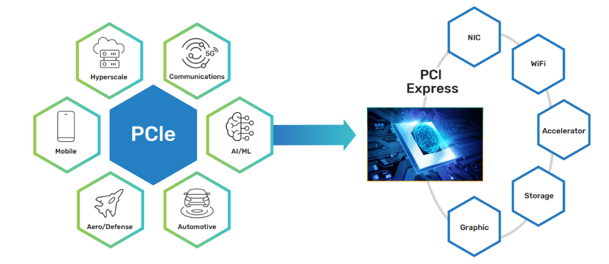
PCI Express (PCIe) has been widely adopted as the primary I/O interconnect since its first debut in 2003 (PCIe 1.0 standard release) in wide breach of applications, from hyperscale, artificial intelligence / machine learning (AI/ML), and aero/defense, to 5G communications, mobile/consumer, automotive, etc. It’s a versatile, high-performance, robust, and mature interconnect standard with full backward compatibility, which enables a solid and strong ecosystem in the industry. This paper discusses how a refined and enhanced PCIe multi-protocol PHY IP block can pave the way to a new approach in SoC architecture and planning with the benefits of shortened TTM and competitive development cost.
Overview
Introduction
In response to the market’s push for higher transport bandwidth, the latest PCIe 5.0 brings the data rate/link speed up to 32Gbps (NRZ signaling) while the next-generation PCIe 6.0 will further push the envelope to support 64Gbps (PAM4 signaling). On the marketadoption front, PCIe 4.0 is slowly becoming real as more and more systems are upgraded and more products are made available in the market. Having said that, PCIe 3.0 is the most mature PCIe interface and is widely deployed as the main interconnection for various types of I/O use cases in tons of applications.
PCIe 3.0 use cases include being used as the interconnect for chip-to-chip (e.g., main processor to accelerator communication) and chip-to-module (e.g., processor to network interface card (NIC)/Wi-Fi and NVMe flash storage) use cases. The latest USB standard, USB4, also incorporates PCIe 3.0 (data transmitted through the encapsulated packets) to enable fast external storage solutions as well as external graphic cards that work as well as one built with the conventional PCIe interface. These are just some common use cases for PCIe, but many other standard/protocols can be adopted in modern SoCs, such as USB (another well-known I/O interface), SATA (interface for HD/SSD drive), DisplayPort/HDMI (for the system require display function), and Ethernet standards, etc.
Creeping Complexity of SoC Development
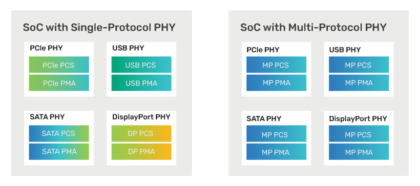
Supporting the growing requirements of different interface protocols means introducing more design blocks, thereby creating more integration and verification complexity, which can be a productivity drag. In some markets (e.g., consumer electronics), managing the changing needs of different protocols or enabling a protocol-configurable system are facts of life that must be addressed in the early phase of architecture development. Each protocol requires a different functional block, adding not only R&D complexity (from design to silicon validation and system bring-up) but operation/procurement complexity (to potentially source different IP from different vendors). By committing at this point, SoC architects can be handcuffed by these limited block choices, forcing them to make tradeoffs too early while sacrificing flexibility and giving up potential markets. This is why we are seeing the rise of using multi-protocol PHY in the industry.
How a Multi-Protocol PHY Works
Typically, a PHY consist of two key components: the physical media attachment (PMA) and the physical coding sublayer (PCS). The PMA is the analog part of the SerDes implementation, while the PCS is a digital block establishing the functional link to the protocol supported. A multi-protocol PHY implements support for multiple protocols by optimizing the usage of the signal-path blocks needed for each protocol. In the case of the PMA, this support consists of a common high-speed SerDes signal path across multiple protocols. For the digital PCS, it entails a configurable design that uses the same signal-path components multiplexed as needed for different protocols. This approach leads to optimized die area and, as a result, lower SoC cost and an accelerated design schedule.
By tapping into a single multi-protocol PHY IP, an SoC designer can reuse many of the common design building blocks, enjoy a much simpler design verification process, and benefit from a faster bring-up and characterization process while only managing one single PHY design.
A Different Approach: Multi-Protocol with Multi-Link Capability
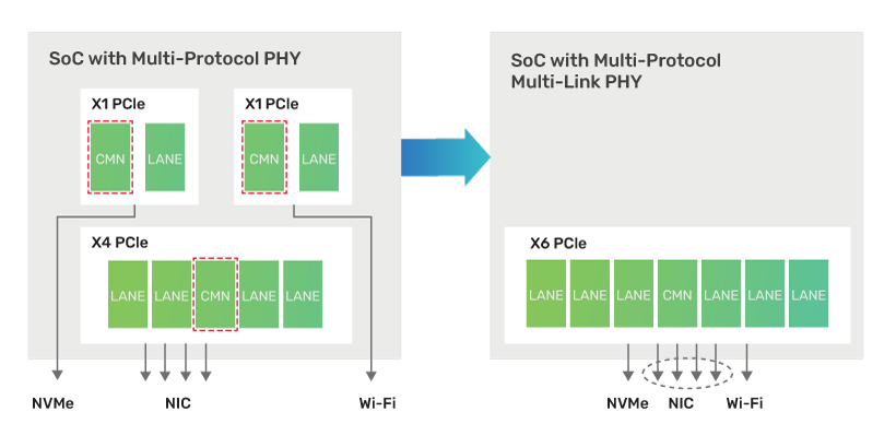
Though multi-protocol PHY IP has gained traction in SoC design teams, there’s a new wrinkle emerging in this paradigm: Independent multi-link in a given multi-protocol PHY, which adds another layer of flexibility for SoC designers.
Let’s illustrate the concept with the following example. A multi-protocol PHY block was meant for an SoC system design requiring the following configuration: one link of a 4-lane (x4) PCIe for NIC interface, one link of a 1-lane (x1) PCIe for NVMe connection, and one link of 1-lane (x1) PCIe for Wi-Fi module interface. The conventional multi-protocol PHY was designed to operate only in a single-link configuration, meaning that a total of three separate PHY instances were required to support a three-link operation. With the new multi-link capability in conjunction with a multi-protocol PHY, multiple links can coexist in a single PHY instance. This adds the flexibility to combine the multiple links altogether in a single PHY instance to gain extra PPA benefit by removing the redundant common building blocks, as depicted in Figure 3.
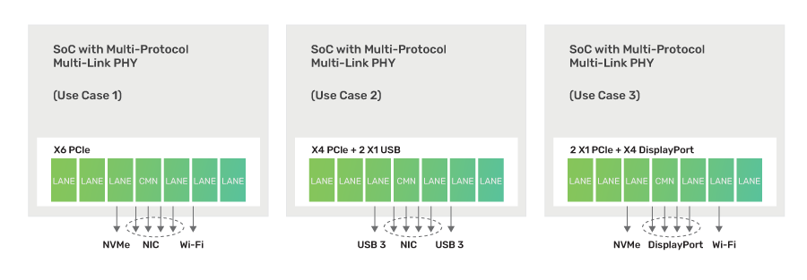
Another typical use case is to mix and match different protocols in a single SoC product, giving the designer the flexibility to change the protocol combinations to address different market segment needs. As shown in Figure 4, the same x6 PCIe PHY (supporting NIC, NVMe, and Wi-Fi) could be re-configured to substitute the NVMe (x1 PCIe) and Wi-Fi (x1 PCIe) with two ports of USB3 (2 x1 USB3). Or replace the NIC interface (x4 PCIe) with DisplayPort (x4 DP), and keep NVMe (x1 PCIe) and Wi-Fi (x1 PCIe) for another type of configuration. Whatever configuration is choosen, the basic circuitry remains the same.
Cadence 10Gbps Multi-Protocol Multi-Link PHY IP
The Cadence 10Gbps Multi-Protocol PHY IP supports a wide range of frequencies, 1.25 – 10.3125Gbps, with the capability to support popular interface protocols, such as PCIe 3.0, USB3.1/3.2, SATA3, DisplayPort TX, and Ethernet. It was specifically optimized for the PCIe 3.0 standard with very low L1 sub-state leakage (in tens of uW range) and ultrafast L1 sub-states exit latency (10us – 25us) for power-efficient applications. This IP is currently available in process nodes from 16nm to 5nm.
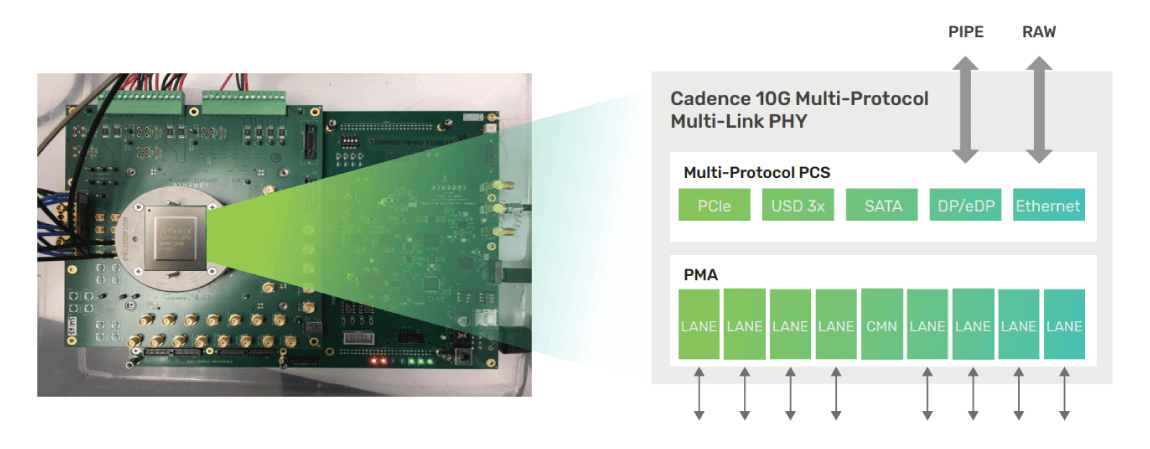
This PHY IP offers two different multi-protocol configurations: single-link and multi-link. Single-link offers a conventional multi-protocol function with all the lanes running one protocol at a time. Thanks to the refined and enhanced clocking topology employed in this PHY design, the multi-link option offers greater flexibility for SoCs to exploit different protocols concurrently via different lanes.
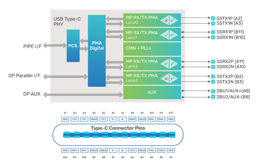
This PHY IP also offers another ease-of-use x4 transceiver configuration, as shown in Figure 6, to handle the popular USB Type-C application that supports USB3.x (x2) with a DisplayPort TX alternate mode. This multi-protocol multi-link PHY IP perfectly addresses the market demands with the following advantages:
-
 Optimum configurability: Provides the flexibility to bridge different protocols such as PCIe, SATA, USB, and Ethernet with single IP design
 - Reduced development risk: Alleviates engineering burden for managing technical complexity of each protocol by handling single IP integration
- Shortened product TTM: Competitive R&D cost along with fast TTM is achieved by sharing common components and reducing the time required to bring up each protocol PHY
Conclusion
Designing SoCs with a multi-protocol PHY IP is one solution to the challenges of balancing different, and continually evolving, interface protocols and addressing the needs of applications that need flexible product configurability. Cadence‘s Multi-Protocol Multi-Link PHY IP gives SoC developers the optimal flexibility to integrate multiple commonly used interface protocols with only a single PHY design. Such an approach saves product development time (faster TTM), reduces the risk of using multiple different PHY solutions (one PHY for all), and provides a flexible configuration to enable different product features/protocols (flexibility to address different market demands).