White Paper
Computational Software
Electronics technology is evolving rapidly, becoming pervasive in our lives. There are more smart phones in use than there are people on earth, driver assistance is now common in automobiles, commercial airplanes have increasingly sophisticated infotainment, and wearable health monitors exist for a plethora of missions. Every device is generating and communicating massive amounts of data, including audio and video, creating an explosion of information. Even with today’s technological innovation, there is not enough network bandwidth, cloud compute, and storage to capture, process, and analyze all this data.
Overview
Introduction
To power the technologies and products of the future, end-application system companies are increasingly designing the full stack of their solution. Some are even designing their own semiconductors, and optimizing the end-to-end solution across chips, packages, printed circuit boards (PCBs), software, and the entire system to meet demanding market requirements. This movement is driving a convergence of three trends in electronics design, as shown in Figure 1. First, many applications require intelligent computation in their systems, optimized for the specific application and workload. Second, advancements in traditional CPU clock frequency have tapered off, constrained by core architectural limitations. Third, Moore’s Law has been driving exponential growth in semiconductor density, producing performance and power benefits when adopting new semiconductor process technologies, but the rate of progress has slowed. In addition, the cost of advanced-process nodes has grown substantially.
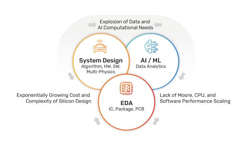
The teams designing these products are under relentless pressure to produce results rapidly and flawlessly. Their challenge is to deliver new, differentiated products faster and more efficiently, despite the growing complexity of both silicon and software and with new challenges such as 3D packaging, integrated intelligent sensors, and 5G radios. Computational software tools address the design challenges of each of the semiconductor, system, and intelligence design dimensions.
Electronic design automation (EDA) has always been driven by advancements in computational software, in applications such as SPICE, layout, synthesis, and static timing analysis. System design requires multi-physics analysis and simulation, a computational software application area. Machine learning in intelligent computation operates on a scale all its own, utilizing recent innovations in pattern-based computation. What is new is the confluence of challenges across these domains, necessitating innovative computational software that spans the full scope of the systems and simultaneously addresses tradeoffs in large scale design.
Creating the best computational software is the key to successful intelligent system design. But it’s not solely traditional algorithm implementation that is enabling huge advances in capability and productivity. This era of computational innovation includes three new trends: the integration and co-mingling of previously independent design, analysis and implementation to achieve optimal results, partitioning and scaling of computation to thousands of CPU cores and servers, and machine learning—a category of artificial intelligence—to improve design heuristics and optimization.
Optimizing Computational Software
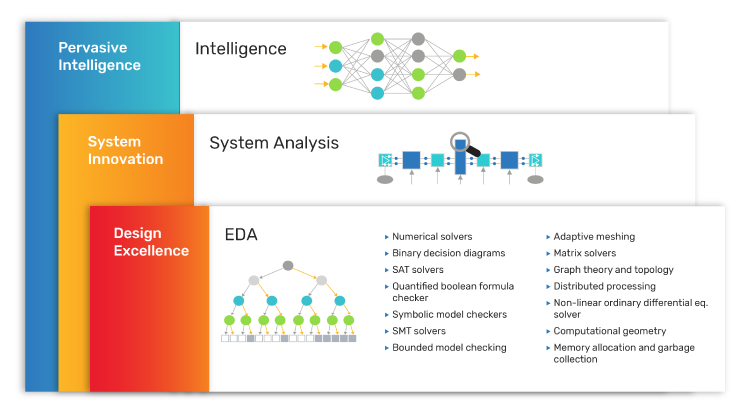
Originating in research labs, universities, and early semiconductor companies, the development of software tools for the design and testing of electronics has enabled engineers to create solutions to address complex design and time-to-market challenges. Many of the core design problems involved are intractable, require a combination of complex algorithms and heuristics to complete in acceptable runtime, and produce suboptimal results. Examples include nonlinear ordinary differential equations and matrix manipulations for analog simulation, combinatory optimization and non-linear equation optimization for digital synthesis and implementation, and compiler technology and solvers such as binary decision diagrams for logic simulation and formal verification used in many EDA tools, as shown in Figure 2.
Each computational innovation yields a new gain in productivity and scalability, often enabled by the introduction of abstraction and automation. Early electronics were all analog, followed by logic gates, but now most large chips are designed with a register-transfer-level (RTL). Many chip design teams are now using SystemC/C/C++ as the design programming language with high-level synthesis. Tools enable designers to create and debug designs and automate the process of transforming the design from the high-level description to the low-level implementation language required for manufacturing. The design flow is implemented in separate phases: simulation, synthesis, placement, routing, physically aware timing/power/area optimization, timing verification, power integrity (EM-IR) analysis, and so on. Computing these analysis steps together can produce better results and reduce iterations in the design flow.
To counter the growth in design size, complexity, and computational scope, the algorithms now utilize multiple CPU cores, and perhaps multiple servers. Characterizing a standard-cell library with hundreds of cells and hundreds of corners can easily make use of 50,000 CPU cores. Other algorithms, like digital back-end implementation due to the amount of shared data and involving multiple simultaneous optimizations, are harder to scale due to the amount of shared data that must be kept synchronized.
One particular high-value area is solving large numbers of simultaneous linear equations, such as Maxwell’s equations for electromagnetic analysis. The algorithms involve partitioning of very large, sparse matrices across CPU cores, and then solving each sub-matrix individually while managing just the right amount of communication among the CPU cores. 3D analysis, finite element analysis, circuit simulation, signal integrity, and even the training of neural networks all use sparse matrices. Techniques to efficiently parallelize and solve sparse matrices across many CPU cores are a core competency of computational software organizations.
A special case is accelerating computational software by implementing the algorithms, wholly or partially, in hardware. An example of this technique is a special-purpose supercomputer technology called an emulator, which mimics the function of a semiconductor chip at high performance, enabling early software development and system debugging from a high-level design description, such as RTL, before the chip is manufactured.
System-Level Computational Software
As the capabilities of the semiconductors increase, designs become more complex and the sensitivity of electronics to environment, signal noise, and other factors grows. Moore’s Law no longer provides the same benefits relative to the increase in cost of moving to a more advanced-process node. Combining chips in a multi-die package provides better cost optimization in many cases.
Electromagnetic analysis became necessary to ensure signal integrity at very high speeds, and nearly all chips have to be designed in the context of, or co-designed with, other chips, connectors, sensors, radios, and PCBs. To enable the finite element analysis algorithms to complete in a reasonable time, engineers used to hand partition the system into small enough pieces to analyze, hoping that the partitions wouldn’t be weak points in signal transmission. This traditional process sacrificed performance margins to ensure quality, due to the lack of closed-loop control over the design.
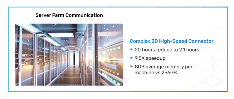
Every aspect of the system depends on the electrical transmission speeds, including size, performance, voltage, power consumption, temperature, radiation, and more. Multiphysics simulation is now a necessity for electronics system designs. One example of the interplay of these traits is high-speed SerDes communication with data rates up to 112Gbits per second— see Figure 3. Here the signals originate on the semiconductor chip, transmit through pins onto a PCB, travel across traces to a connector via a cable and on to some other system component, eventually reaching another semiconductor chip. This entire path must be analyzed and optimized for the signal requirements. Another example is with certain 5G radio-frequency (RF) designs where the signals exit the PCB and transmit via an antenna.
In addition to analysis, it’s important to speed time to market. The complexity of systems requires co-design and co-optimization of the semiconductor with its IC package, PCBs, connectors, and cables. This requires shared data and integration of algorithms to compute the best design choices across the overall system. Therefore, analysis tools need to be connected with those chip/package/module/PCB design environments to enable automated selection of optimal system implementation decisions.
Machine Learning Optimization
One of the long-running challenges in applying computational software to electronics design is finding the right formula or process flow. Design tools and designers often apply recipes, or ordered sets of steps, when applying computational algorithms to their design challenge. Each of these algorithms works to find the best answer—balancing quality of results, runtime, and memory—for its part of the overall problem. As system design complexity has increased, design heuristics in software tools and flows are less able to produce optimal results.
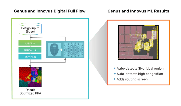
Machine learning technology is particularly good at large-scale, pattern-based algorithms, and is implemented with the same matrix analysis technology found in EDA and system analysis. By repeatedly applying computational design algorithms, such as circuit layout or PCB placement and routing, tools can evaluate thousands of possibilities and the best outcome can be selected. Machine learning is well suited to this type of problem as these tools evaluate and learn from successful prior designs, allowing them to identify optimal choices for new designs—see Figure 4.
And while machine learning at the chip level is about optimizing chip design, at the system level it can also be applied to how the chips and system are decomposed and designed to meet optimal overall design requirements. Even the settings for system-level extraction and simulation tools can be tuned for optimal convergence and performance for a given design challenge utilizing machine learning. Importantly, this creates even more value in a unified data infrastructure to deploy integrative analytics.
Summary
Computational software is emerging as a driving force to enable innovative solutions for the multi-billion-dollar electronics systems industry. What’s different about this era of computational software centers on three key innovations:
-
 Integration and co-mingling of previously independent design, analysis, and implementation to achieve optimal results,
 - Partitioning and scaling of computation to thousands of CPU cores and servers, and
- The introduction of machine learning to improve and harness design heuristics for system optimization.
Cadence, a computational software company, is leveraging our algorithmic expertise to expand beyond the EDA market into system analysis, machine learning, and other domains (Figure 5).
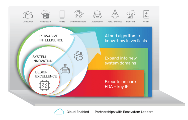
Cadence has evolved to address key industry changes and has formulated its Intelligent System Design strategy for delivering world-class computational software capabilities for the design of intelligent electronic systems. We’ve created a culture of innovation in computational software—hiring top talent, nurturing growth, inspiring creativity, and rewarding results—to realize our vision.
Our goal is to empower engineers at semiconductor and systems companies to create innovative, intelligent, and highly differentiated electronic products that transform the world. We enable designers to unleash their imagination by addressing the complex computing demands of artificial intelligence, 5G, and high-performance computing, resulting in pervasive intelligence across autonomous vehicles, industrial IoT, advanced data centers, health, aerospace, and more.