In the domain of electronic product design, solely relying on process shrink as the primary driver of product innovation and improved system performance is no longer a viable approach. The cost and complexity associated with advanced nodes has everyone looking for alternatives to the traditional monolithic system on chip (SoC). The path most are taking leads to the world of “More than Moore” and heterogenous integration. These heterogenous, multi-chiplet architectures provide a much lower cost alternative to the latest design nodes, while still providing a robust re-use model based on IP in the form of physically realized chiplets. The package design now sits in the center of the universe for the next generation of electronics.
Introduction
In the domain of electronic product design, solely relying on process shrink as the primary driver of product innovation and improved system performance is no longer a viable approach. The cost and complexity associated with advanced nodes has everyone looking for alternatives to the traditional monolithic system on chip (SoC). The path most are taking leads to the world of “More than Moore” and heterogenous integration. These heterogenous, multi-chiplet architectures provide a much lower cost alternative to the latest design nodes, while still providing a robust re-use model based on IP in the form of physically realized chiplets. The package design now sits in the center of the universe for the next generation of electronics.
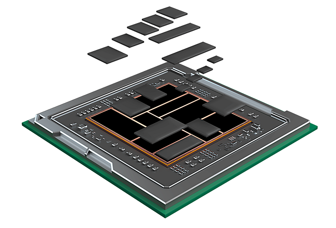
The semiconductor packaging industry is now poised to take on a larger, more significant role in electronic product design of the future. To meet the market demand for these heterogenous, chiplet-based architectures (Figure 1), new system-level design methodologies are required, targeting system-level power, performance, and area (PPA). When designers transition from single monolithic devices to multi-chiplet architectures, the first challenge they face is how to plan, manage, and optimize their top-level design and connectivity. A novel system-level design management solution is now required. This platform must be capable of aggregating data from the integrated circuit (IC) designer, the package designer, and even the board designer, for the purposes of system-level optimization and providing the top-level netlist for signoff connectivity verification.
Other challenges arise for the traditional package designer. The biggest challenge can be the transition from expertise in layout of laminate substrates to layout of silicon substrates. In addition, silicon substrates (masks) require a formal physical verification process that is new to most of today’s package designers.
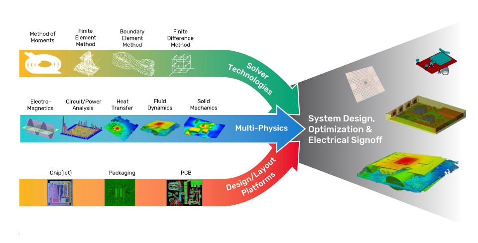
And we can’t forget about the electrical and thermal analysis challenges that will arise. Here again, these tools have to provide value at the system level. To do this, the tools have to support in-design and electrothermal signoff, for on-chip and off-chip devices and interconnect (Figure 2). Cross-domain coupling effects must also be modeled.
When it comes to chip(let)-level thermal analysis, typically an on-chip(let) EM-IR solution is required to produce a detailed thermal model. This chip(let)-level thermal model is then consumed by a system-level thermal analysis solution to include the packaging and PCB (the largest natural heat spreader) along with any heatsinks in the design. The system-level thermal tool then provides the engineer with thermal gradient information as well as thermal stress calculations. Additionally, an updated chip(let) thermal map is generated. This map can then be fed back into the chip(let)-level EM-IR tool, which can then more accurately perform chip power analysis and IR drop analysis. Here again, the importance of modeling at the system level is paramount.
To summarize, the slowdown of Moore’s Law was well anticipated and prompted many leading-edge companies to look towards going beyond it. Recouping non-recurring engineering (NRE) costs for low-volume chip production when designing a complex SoC at the latest node became almost impossible for small-scale companies. Department of Defense (DoD) companies realized this early and are leading the way in finding design alternatives for single monolithic SoCs. Today’s advanced IC packaging is about adding value to end products and contributing to improved PPA. Electronic product design companies are leveraging packaging technologies to create value and differentiation from their competitors, with multichip(let) solutions focusing on a “More than Moore” vision. In other words, when cost and low volume came into play, the system in package (SiP) became the ideal alternative to designing an advanced-node monolithic SoC. Gordon Moore foresaw this possibility of the disaggregated design approach and predicted that “It may prove to be more economical to build large systems out of smaller functions, which are separately packaged and interconnected.”
Chiplets and Heterogeneous Integration
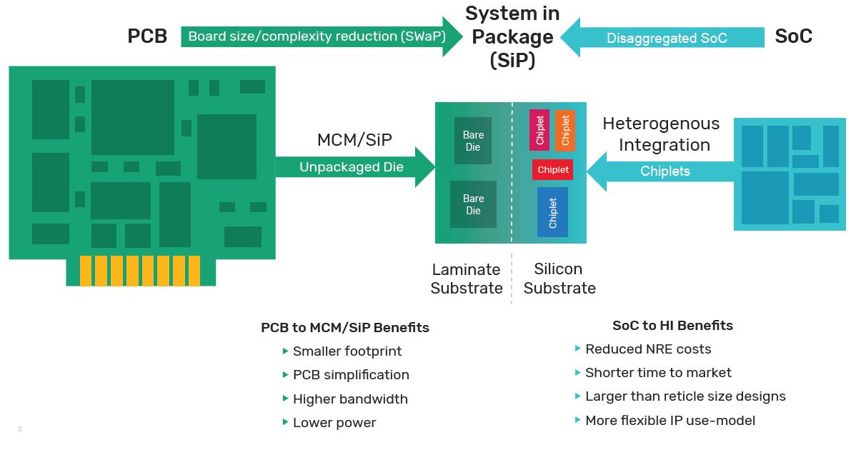
A chiplet is a physically realized and tested (hardened) IP with a standard communication interface manufactured in a silicon wafer to reduce cost by increasing the manufacturing yield and reusability across applications. The chiplet-based architecture allows designers to leverage IP without regard to the node or technology on which it is manufactured. Designers can focus solely on their IP or the value-add they bring to the design. These chiplet-based designs can be built on different materials such as silicon, glass, and even laminate. The result is a high-performance pseudo-SoC built at a lower cost in less time. The reusability of chiplet helps in cost reduction during design and improving yield.
The term “heterogeneous integration” has been widely adopted to describe a disaggregated SoC architecture built from multiple chiplets (Figure 3). A chiplet-based design is like a SiP except for multiple IP in the form of chiplets are integrated on a single substrate instead of the usual SiP approach of integrating multiple bare dies (including 3D stacking) on a single substrate. But it is also similar to designing a small PCB, as each chiplet will be built with a common/known communication interface such as PCI Express® (PCIe®), HBM, or AIB. The value proposition that heterogeneous integration offer is:
Many leading semiconductor manufacturers are exploring this space. The Intel CO-EMIB heterogenous packaging platform allows deploying EMIB and Foveros together in the same package. Intel Omni-Directional Interconnect (ODI) allows top-packaged chips to communicate with other chips horizontally, similar to EMIB, or vertically, through TSVs, similar to Foveros. TSMC’s Chip-on-Wafer-on-Substrate (CoWoS) is another platform for heterogeneous integration.
Where Do We Go from Here?
Even though designs are being built today with multiple chiplets, most chiplet-based designs are developed at vertically integrated companies that are designing both the chiplets and the modularized or disaggregated SoCs. To move chiplet-based architectures into the mainstream, chiplets need to become widely available, and the vision of commercialized chiplets will require IP providers to devise a suitable business model. One way to propel this vision is the development and documentation of chiplet standards, such as I/O pitch, communication interface and corresponding “compliance kit,” and thermal power model. Several organizations, including U.S. government programs and standards bodies such as Open Compute Project/Open Domain-Specific Architecture (OCP/ODSA), are actively working towards closing the chiplet gap.
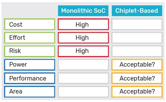
It is exciting that the ecosystem is changing. Large semiconductor foundries are now offering their versions of advanced packaging, and many ways of supporting design teams like reference flows and process design kits (PDKs) are becoming part of the design environment. These concepts have been typically lacking in the packaging community as a whole. Cadence has worked with many of the leading foundries and outsourced semiconductor assembly and test companies (OSATs) to develop multi-chip(let) packaging reference flows and package assembly design kits. The acceptability of lower performance, higher power consumption, and a larger area of chiplet-based architectures by a generation of SoC engineers who have put in tremendous value on the ideal PPA (Table 1) is still a question that we need to wait and watch.
The Evolution of Chiplets
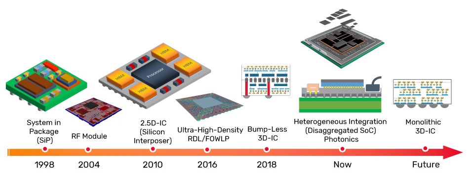
The transition to a chiplet-based architecture is a more subtle change if you consider the evolution of semiconductor packaging over nearly five decades (Figure 4), with heterogeneously designed integrated multi-chip products along for most of that time. EDA companies started to develop tools for advanced packaging in the early 1990s, around the time the ball grid array (BGA) provided a high-performance, small form-factor option to the mechanical lead frame package.
Multi-chip modules (MCM) date back to the 1960s, which is still common for some applications. The term SiP began to replace the term MCM in the late 1990s as wafer-level testing became ubiquitous, and the KGD problem that plagued MCM design started to become less of an issue. This is also about the time that package designers started stacking die, which clearly shows that 3D stacking is not new to package designers. In the early-mid 2000s, RF modules started to move to the laminate BGA packages that are very common in today’s smartphones and watches. Moving to the current generation of advanced multi-chip packaging, silicon substrates now provide a high-density alternative to organic substrates with the introduction of through-silicon vias (TSVs). The earliest example of leveraging TSV-based silicon interposer technology was the re-partitioned Xilinx FPGA. Today, this technology is most commonly referred to as 2.5D-IC packaging.
Ten years ago, semiconductor foundries extended back-end design into silicon-based advanced packaging solutions. The foundry-based approach of high-density RDL also drove renewed interest in fan-out wafer-level packaging (FOWLP) and now, with support for multiple dies, interest is at an all-time high. Additionally, to further increase bandwidth, 3D-IC packaging, meaning wafer-on-wafer or chip-on-wafer stacking, has a new life.
The chiplet trend (Figure 4) shows that next-generation chiplet-based technologies are just a new way of partitioning logic that aligns nicely with advancements in package manufacturing technologies.
Tools and Flows for Heterogeneous Integration
The transition to a chiplet-based approach introduces new challenges in EDA tools for both chip designers and package designers. Package designers are required to familiarize themselves with requirements such as layout versus schematic (LVS) and smart metal balancing for performing layout and verification of silicon substrates. Chip designers must handle requirements for defining and managing top-level connectivity when moving from designing a single device to designing and/or integrating multiple devices. Testing is another area that changes significantly when designing multiple chiplets in a 3D stack. For example, testing the chiplet in the top of the stack that may not have any connections to the outside world. The bottom line is that laying-out and verifying designs with multiple chiplets will introduce new challenges for both the IC design team and the package designers. Design tools and methodologies that have been extended to support multiple chiplets play a crucial role in the success or failure of the project.
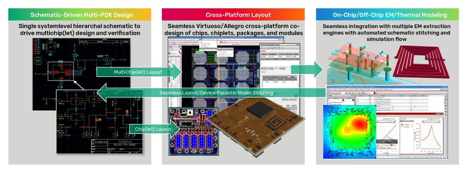
From an EDA tool provider perspective, it is important to develop cross-domain design flows that provide users with a platform to seamlessly plan, design, analyze, and verify across chiplet, interposer, package substrate, and board. This platform should provide many unique capabilities for designing multi-chiplet-based packages (Figure 5), starting with a single logical hierarchical representation of the complete multi-chiplet design, from the transistor level of each chiplet up to the full system-level design. This system-level schematic is the basis for seamless LVS and functional verification that ideally includes layout parasitics across chiplets, interposers, and package substrates. It should even extend to the PCB if the user desires.
A novel approach to chiplet/package co-design can also be enabled as part of this holistic, system-level design platform. Finally, multiple electromagnetic field solvers, including finite element method (FEM) and method of moments (MoM), must be integrated into the flow, allowing streamlined device modeling and layout parasitic extraction for both on-chiplet and off-chiplet geometries. There should be automation that seamlessly stitches the electrical models back into the golden hierarchical system-level schematic. Such a platform would provide designers with an easy way to transition into the world of chiplet-based architectures.
Conclusion
From the system-level design framework discussed above, the user should be able to design and/or import multiple chips or chiplets across any technology or node. The designer would then instantiate each chiplet schematic symbol into the top system-level schematic, where additional package-/board-level devices could easily be added from the system-level library. This schematic serves multiple purposes, including system-aware functional simulation, and maybe most importantly, it provides the golden netlist required to perform LVS checking of the complete system-level design. This methodology gives the designer system-level signoff confidence at the same level they have when signing off on their chiplet.
