- Overview
- Tensilica Xtensa Configurable Processors
- Introducing HW accelerators presents a set of unique design challenges
- Stratus High-Level Synthesis
- Example – PPA Improvement through TIE and HW Accelerator Design
- Pure Software AES Performance Analysis
- Xtensa Processor and Software Modification
- Stratus Import
- Accelerator Testbench Creation
- Accelerator Optimization
- Summary of Results
- Conclusion
White Paper
Automated HW/SW Co-Design of DSP Systems Composed of Processors and Hardware Accelerators
Seemingly overnight, data acquisition and digital signal processing have gone from a hidden background function in special purpose-built subsystems, such as PC graphics cards and airborne missile guidance systems, to the foreground in the form of in-ear IoT devices, smartphones, and autonomous vehicles. As the number of smart data-acquisition devices grows, so does the amount of data requiring digital signal processing—compression, encryption, signal conditioning, etc.
Overview
Overview
To improve performance and reduce power and cost, designers are moving from processors to systems composed of processors with companion hardware accelerators. Design decisions such as HW/SW partitioning and hardware accelerator micro-architecture tradeoffs present unique challenges because many PPA details aren’t available until well into the design implementation phase. Without this detail, designers use inaccurate estimates and often fail to produce optimal designs. This paper discusses an integrated solution composed of a Cadence Tensilica Xtensa configurable processor and Cadence Stratus High-Level Synthesis (HLS) tool that enables the automated design of PPA-optimized systems of processors with companion hardware accelerators. The solution delivers the following benefits over conventional manual approaches:
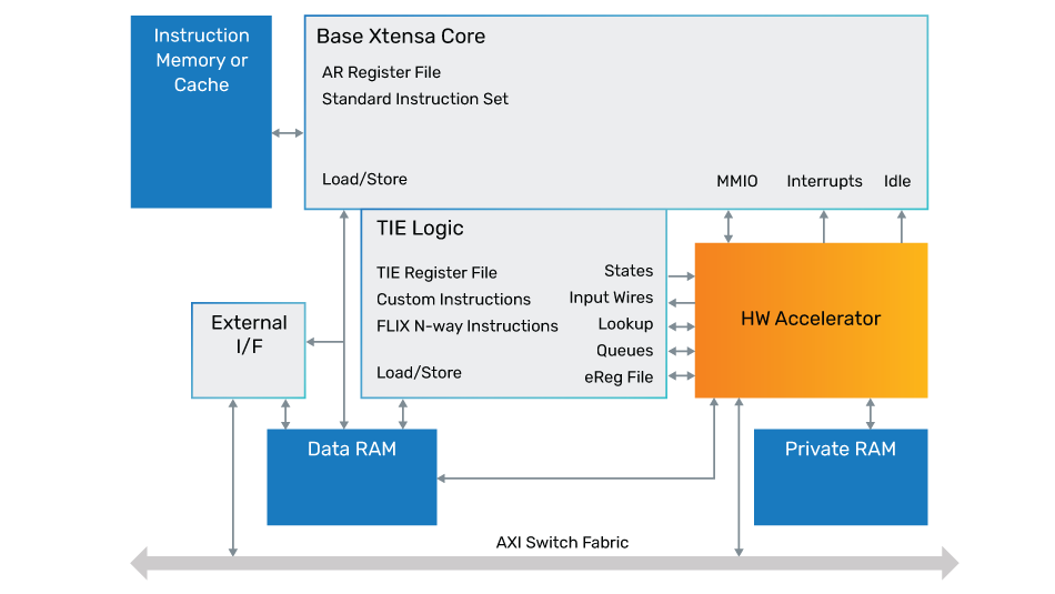
Figure 1: Simple block diagram of Xtensa architecture
-
 Rapid PPA measurement-driven HW/SW partitioning
 - Automated processor/accelerator interfacing
- Automated generation of RTL for the HW accelerator
Tensilica Xtensa Configurable Processors
Tensilica Xtensa configurable processors feature pre-defined configuration options that give control over numerous features, including the memory subsystem, debug, and interrupts. Additionally, custom instructions, execution units, and processor I/O interfaces can be added to match the needs of your application.
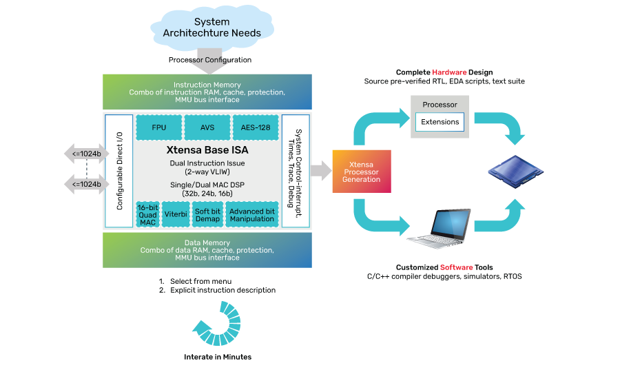
Figure 2: Xtensa configurability
The Xtensa Processor Generator supports rapid configuration and software development as all configuration and instruction changes remain completely compatible with the existing software ecosystem.
Companion hardware (HW) accelerators may be designed for even greater performance or power savings.
Introducing HW accelerators presents a set of unique design challenges:
- How to partition HW/SW for optimal PPA
- How to measure PPA for candidate SW partitions and HW architectures
- How to design power-saving techniques such as power- and clock-gating
- Which power-saving techniques to apply to lower power consumption while meeting performance requirements
- How to design and optimize the HW accelerator micro-architecture for optimal PPA
Stratus High-Level Synthesis
Stratus HLS addresses these challenges. Stratus takes an abstract C++ design description and automates micro-architectural exploration and optimization yielding a PPA-optimized RTL description.
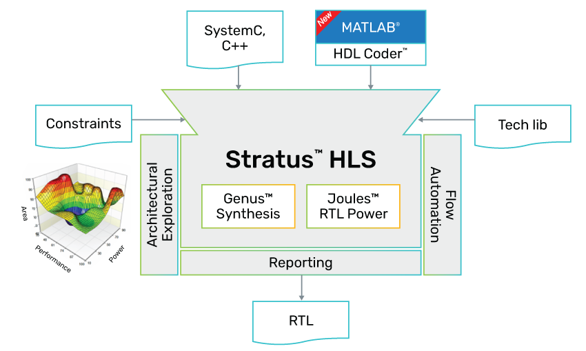
Figure 3: Stratus HLS
By integrating Stratus HLS with the Xtensa Processor Generator, the aggregate solution enables performance-based HW/SW partitioning and automated HW accelerator micro-architecture exploration, optimization, and RTL production. The integrated flow provides very high productivity gains that allow users to implement and measure the impact of HW/SW tradeoffs rather than using estimates. This delivers on the promise of true HW/SW co-design.
Example – PPA Improvement through TIE and HW Accelerator Design
When designing processor-based systems, several components must be optimized to achieve the best overall end-system performance:
1. Software – modifications performed to improve performance considering the processor’s resources and I/O characteristics.
2. Processor instructions and resources – selecting a processor and configuring instructions and resources that best meet the application's needs.
3. HW/SW partitioning – partitioning functionality across the processor and hardware accelerator to best achieve system performance and power goals.
4. Hardware accelerator micro-architecture – designing the hardware accelerator micro-architecture that best achieves performance, power, and area goals.
5. Memory and interfaces – designing memory subsystems and their interfaces to achieve system performance goals.
Xtensa processors and tools support software profiling and optimization, instruction, and resource extensions and offer flexible memory and interface configurations. Existing Xtensa documentation details these capabilities, as they relate to items 1, 2 and 5 above. This paper and the following example focus on the integrated Stratus and Xtensa solution that supports measurement driven HW/SW partitioning and hardware accelerator design from an abstract C++ function—items 3 and 4 above.
An example illustrates the benefits of the integrated Stratus and Xtensa solution. The example presents multiple approaches for implementing an AES encryption algorithm. We begin with an AES encryption algorithm running on the processor as a pure software implementation. We can measure the performance of the overall solution (i.e., an Xtensa processor performing a sequence of AES encryption steps) in terms of processor clock cycles used to complete a specific task. We then examine an alternative implementation of the encryption function in a hardware accelerator using the Xtensa processor to move data and orchestrate the overall flow. We measure the performance of this system (i.e., a combination of processor + software + hardware accelerator) in the same manner as the pure software implementation. Figure 4 through Figure 6 illustrates the different implementations, and we discuss the details of each implementation approach below. For comparison, Table 1 summarizes the results and time required for implementation.
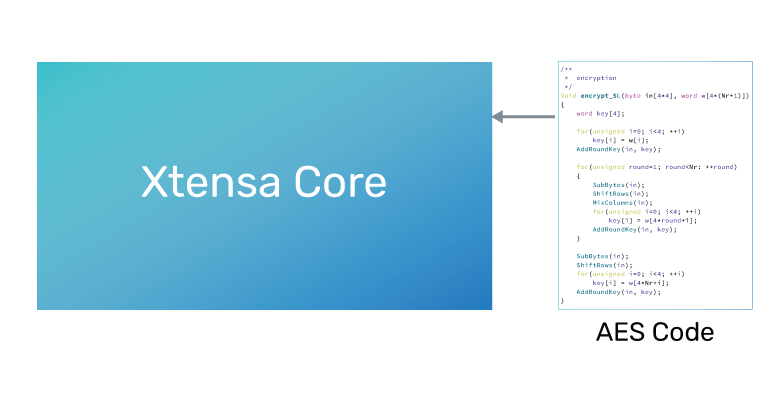
Figure 4: Implementation 1 - AES in pure software
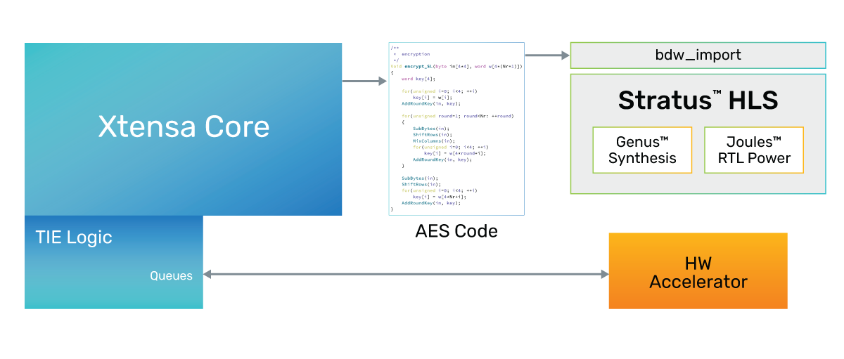
Figure 5: Implementation 2 - AES in HW accelerator
In this example, we focus on an AES encryption algorithm to demonstrate the improvement in run-time performance and silicon area. The critical steps in building our two implementations are as follows:
- Implementation 1 – Pure software AES (Figure 4)
- Configure the Xtensa processor
- Implement an AES algorithm in software to run on the Xtensa processor
-
- Implementation 2 – Hardware accelerator AES (see Figure 5)
- Configure the Xtensa processor, but use TIE to add QUEUE and wire interfaces used to communicate with the external HW accelerator
- Implement the HW accelerator
- Modify the software running on the core to remove the AES code and pass the data off to the external accelerator
-
This example shows how the integrated solution delivers dramatic productivity improvement vs. manual accelerator definition, system configuration, and analysis.
Pure Software AES Performance Analysis
We begin by measuring the performance of the pure software AES algorithm running on the Xtensa processor. The Xtensa Xplorer Integrated Development Environment (IDE) allows you to view the profiling results generated by the Tensilica pipelineaccurate ISS. Using the Xplorer IDE, we measure the performance of the pure software AES algorithm at 270k clock cycles for 128 encryption steps.
Xtensa Processor and Software Modification
Reconfigure the Xtensa processor to include ports for input and output queues used for passing data to and from the external AES accelerator. These queues will be connected to the AES accelerator. In addition, the software running on the processor must be modified to remove the AES algorithm code and replace it with code that reads and writes data to and from the newly added queue ports. This will pass data to the external accelerator and read the results back to the processor.
Stratus Import
The AES algorithm code that we removed from the Xtensa core is reused in this step. We take this behavioral C++ implementation of the AES algorithm and run it through Stratus’ bdw_import utility, which will:
- Create SystemC wrappers around the C++ algorithm. This adds hardware-required constructs like clock, reset, and communication ports
- Create a stub testbench for the new accelerator
- Create a Stratus project configuration file
The designer will then modify the Stratus project file to specify parameters such as clock frequency, reset mode, and technology libraries.
Accelerator Testbench Creation
The Stratus bdw_import function creates a stub testbench, which requires user modification to define functional tests for the HW accelerator. The testbench should include reset, I/O handshaking, input stimulus, and expected results.
Using a testbench at this point is not required; however, it allows the user to test the AES hardware implementation independently of the Xtensa core and automatically simulate and gather event activity for power analysis using Stratus’ Joules RTL power analysis integration.
Accelerator Optimization
Identifying an optimal micro-architecture requires design space exploration. Exploration is the process of applying optimization settings and constraints and performing HLS optimization and execution of a user-defined tool chain to perform various analyses (e.g., Genus logic synthesis for timing and area, Joules for power analysis, etc.).
With our chosen technology library and a specified clock frequency of 500MHz, the initial Stratus implementation yields a design requiring 313 processor clock-cycles for 128 encryption steps at a silicon area cost of 19k square microns. While this implementation is four orders of magnitude better than the processor-resident implementation, we observe that the processor supplies 1 input every 2 clock-cycles in this implementation. This corresponds to an input initiation interval of 2 (II-2) vs. the default II-1. As pipelining with Stratus is fully automated, you can simply redefine the pipelining initiation interval constraint to 2 and re-run Stratus. The II-2 implementation does not affect performance but allows Stratus to perform more aggressive resource sharing, resulting in an area of 11k square microns. The complete turnaround time for this new implementation was 20 minutes, demonstrating a significant productivity improvement over hand-coding the RTL.
Continuing our design space exploration to improve system performance, we experiment with a different mechanism for communication between the Xtensa core and the hardware accelerator. Experimenting with new interfaces in Stratus is extremely productive, and the coding changes are minimal.
In this case, we explore a shared memory architecture with two memories—each with two banks. This shared memory architecture removes a performance bottleneck in accessing the memory and should deliver improved performance. This change requires a small SW change (on the processor), as we must fill the shared memory before initiating the encryption step (as opposed to writing and reading the queue interfaces). Figure 6 shows this architecture as follows:
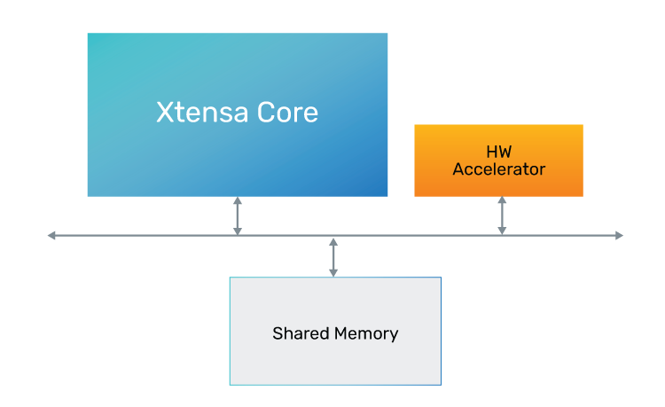
Figure 6: HW Accelerator communicating via shared memory
Performing HLS optimization with these changes (i.e., II-1, shared memory interface) results in the highest performance implementation of 141 processor clock-cycles for 128 encryption steps. This comes at a small area increase to 20k square microns vs. the previous 11k square microns for the TIE-queue-based architecture.
Summary of Results
| Description | Interface Scheme | Pipeline Initiation Interval | Clock-Cycles | Hardware Area (sq. um) | Implementation Time |
|---|---|---|---|---|---|
| Pure software AES | NA | NA | 270,000 | 0 | 3 days |
| Initial HW accelerator | Queue | 1 | 313 | 19K | 1.5 days |
| 2nd HW accelerator | Queue | 2 | 313 | 11K | 20 minutes |
| Fast HW accelerator | Shared Memory | 1 | 141 | 20K | 1 day |
Table 1: System implementation trade-offs + productivity
Our explorations have yielded four architectures with a wide range of performance and silicon area costs. Now the system designer can determine the architecture that best meets their system requirements. The implementation time of these different scenarios is very low and significantly less time-consuming than hand-coding a single RTL implementation. We did compare these HLS implementations to a hand-coded RTL implementation (with II=1) of the accelerator, and the Stratus implementation was marginally smaller. This is consistent with what Stratus users typically report with respect to productivity and PPA vs. hand-coded results—Stratus delivers significant productivity gain with equal-to or superior PPA.
Conclusion
One of the most important values that Stratus customers tout is the ability to explore different micro-architecture implementations easily—putting this capability into the hands of Xtensa users, along with tool automation and compatible interface classes, multiplies that value. Xtensa users are generally more experienced in writing C++ than RTL, so the ability to quickly move parts of their software algorithms, described in C++, off the processor, and implement them as hardware accelerators in RTL, adds a whole new dimension to overall system design. Rather than trying to guess the impact of such HW/SW partitioning tradeoffs, users can actually implement and measure the impact of their HW/SW partitioning candidates.
The Stratus and Xtensa integration is a major step toward true hardware-software codesign. Users can quickly move “the slider” back and forth between HW and SW domains and choose the best implementation that meets their needs based on precise PPA measurements.