White Paper
Accelerate Adoption of High-Speed, Low-Latency, Cache-Coherent Standards Using Formal Verification
We continue to see huge growth in data and compute demand, fueled by increased global data traffic with the 5G rollout , the prevalence of streaming services, and expanded artificial intelligence and machine learning (AI/ML) applications. Several new industry-standard specifications have emerged in recent years to define the protocols of the underlying electronic components and IP building blocks. The Compute Express Link (CXL) 2.0 specification by the CXL Consortium is one such standard defining high-speed, low-latency, cache-coherent interconnects based on the PCI Express (PCIe) 5.0 protocol. In this white paper, we will examine how formal verification techniques have been successfully deployed to verify the implementation of Cadence design IP for these emerging standards.
Overview
Introduction
The cloud computing revolution and proliferation of mobile devices is increasing data traffic and driving changes in data center device architecture. Data-centric applications require high-speed, low-latency communication within and between servers, storage, and accelerators with increasing portions of the memory hierarchy being brought into the coherency domain. The CXL specification is based on PCIe 5.0 and is an open industry-standard interconnect offering high-bandwidth and low latency.
The complexity of these standards, and the effort to architect, design, and verify these IP building blocks for the SoCs of tomorrow, requires innovative techniques to help break down the design and verification challenge into smaller sub-tasks that ultimately contribute to the overall success of the product.
The Cadence IP Group has been deploying assertion-based verification (ABV) techniques for several years to target key building blocks of the PCIe controller product line. Formal verification techniques have been widely used in developing the M-PCIe, cache coherent interconnect for accelerators (CCIX), PCIe 4.0, PCIe 5.0, PCIe 6.0, and CXL 1.1/2.0 controllers.
For complex IP such as PCIe and CXL, it is a question of using all the tools at our disposal to develop the IP: assertion-based formal verification, coverage-driven verification with Cadence Verification IP (VIP)-based Universal Verification Methodology (UVM) environments, accelerated VIP, Cadence SpeedBridge Adapter-based verification on the Cadence Palladium Enterprise Emulation Platform, and FPGA-based prototyping and test chips.
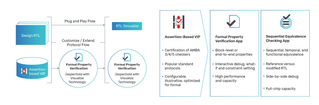
In this white paper, we provide insight into how ABV and the Cadence JasperGold Formal Verification Platform and Apps prove complex modules of the latest Cadence Controller IP for PCIe/CXL, describing how formal verification can accelerate sub-module verification for evolving standard-based design IP.
We also will demonstrate how formal verification metrics can be used alongside traditional coverage-based verification metrics from a UVM-based testbench environment.
Definition of “Formal”
First, a point on terminology regarding “formal” is worthwhile. It is important to distinguish between ABV, the subject of this white paper, and logic equivalence checking (LEC) that engineers within the electronics community may also refer to as “formal”.
A LEC flow compares, for example, a synthesis netlist to the original RTL code. In this case, we are using a tool such as Cadence’s Conformal Smart Logic Equivalence Checker, to formally prove that two design input sources are logically equivalent, e.g., a netlist and the RTL. This flow is particularly useful for engineering change order (ECO) updates to design blocks.
Formal verification using assertions however, is different. In this flow, assertions describe the intended operation of the block under test. The assertions, such as SystemVerilog Assertions (SVA), can be written to describe the expected input to the block (assumptions and constraints) and the expected operation and outputs of the block (checks). In this case, we are using the JasperGold platform to exhaustively analyze the design and check that it always adheres to the rules outlined in the SVA. Note that the JasperGold platform also has the capability to compare two designs using the Sequential Equivalence (SEQ) App.
Why Not Just Use UVM?
This white paper provided a simple answer in the introduction. We are looking to divide and conquer by breaking up a very complex protocol and complex development challenge into smaller sub-blocks to verify at module level.
The Cadence Controller for PCIe and CXL verification environments makes extensive use of the official Cadence VIP for PCIe and CXL, developed by an independent Cadence group to the Cadence Design IP. These VIP-based environments test the full protocol layers of the PCIe and CXL spec, modeling the transaction layer, data link layer, logical physical layer, and PHY layers. The UVM-SV VIP-based environments are critical to the development of the IP.
ABV environments are complementary to the UVM environments and, in some cases, are used to formally sign off blocks.
If we take the CXL controller example, we are implementing a design based on PCIe 5.0, a specification that is over 2000 pages. The CXL 2.0 specification itself is over 600 pages.
Evolving Adoption of Formal for PCIe
The adoption of SVA and property specification language (PSL) assertions in the Cadence controller for PCIe can be traced back to the PCIe 1.0 controller developed in the early 2000s.
PCIe 1.0 Controller
Originally, keen designers developed such assertions directly in the RTL code to quickly flag unexpected or undesired behavior in their own RTL, at source. A good example of such an assertion would be the detection of a buffer overflow in the middle of the PCIe transaction layer:
*E: “TL Buffer Overflow – Inbound Posted Queue”
The designers writing the assertions in the PCIe 1.0 controller wanted an immediate error indication for the issue in their block, rather than potentially waiting many cycles for an end-to-end scoreboard to flag a generic “data mismatch” error.
ABV use evolved at Cadence since the sporadic use of design assertions in the early 2000s. It moved to a more structured approach for subsequent PCIe projects, with ABV forming part of the vPlan within the vManager Metric-Driven Signoff Platform and contributing to coverage metrics.
M-PCIe Controller
In 2012, Cadence verified the standalone Link Training and Status State Machine (LTSSM) of the Cadence M-PCIe controller using formal verification with assertions mapped to a vPlan alongside regular functional coverage (Covergroups), developed using SystemVerilog. The focused effort at the module level identified issues in a shorter space of time than initial end-to-end top-level simulation environments would have.
Cadence presented a paper at the 2013 PCI-SIG Developers Conference entitled “M-PCIe Implementation Case Study.” This paper contained a section outlining the use of formal verification techniques to verify the new M-PCIe LTSSM block, with the key challenge being the early availability of a new LTSSM design block, ahead of full VIP availability.
There was a desire to test the new complex State Machine at module level, while Cadence developed the official VIP and top-level simulation testbench for M-PCIe.
The paper also outlined the formal verification work performed by the controller team:
-
 Early pipe cleaning of new LTSSM RTL code possible with formal verification
 - ~300 assertions developed at block level (some using common properties)
- Shorter time to first passing test once VIP integrated into top-level simulation testbench
- Assertions and constraints used for formal verification are reused in dynamic simulation
CCIX Controller
In 2016, Cadence developed the CCIX controller following the CCIX 1.0 Consortium Specification. For this development, designers extensively used formal verification to verify and sign off the new CCIX transaction layer in parallel to the standard module-level simulation techniques.
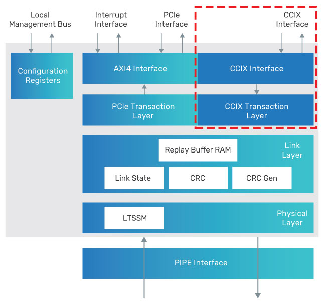
The CCIX formal work focused on the new CCIX transaction layer and host interface, highlighted by the red box in Figure 2 CCIX Controller Block Diagram.
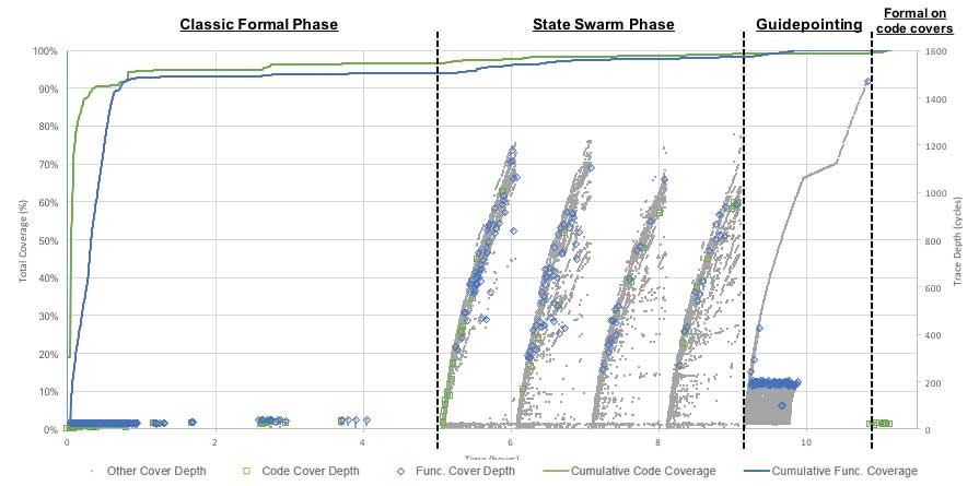
The CCIX formal project found that classic formal verification was the most efficient mode for finding bugs, as demonstrated by Figure 3 CCIX Controller Coverage (2017). However, The JasperGold deep bug hunting modes were also used to efficiently reach deep areas of state space. Coverage was then used to get to planned scenarios that were required for signoff, with the team making extensive use of state-swarm to improve coverage and guidepointing to get to 100% coverage. Designers used soak to search for deep, unplanned scenarios, running formal with no time limit (run until manually stopped), but with coverconstraints to avoid unproductive search paths.
Figure 3, presented by Anish Mathew from Cadence at the Jasper User Group 2017 conference, demonstrated the progress made towards coverage closure using classic, state swarm, and guidepointing techniques.
Key metrics from CCIX transaction layer:
- Registers: 9331
- Gates: 56K
- RTL Lines: 25K
Key points from the CCIX Controller formal signoff work:
- Formal does a better job on short scenarios, simulation a better job on long scenarios
- Formal’s ability to hit more corner cases has side effects—some aspects of the design end up being more robust than necessary, but sometimes unrealistic scenarios are hit and it is hard to constrain them away
- Difficult to write end-to-end checks in formal, especially when considering error/abort scenarios
- The effort to close coverage is comparable between formal and simulation for CCIX transaction layer
The successful use of formal verification through PCIe 1.0, M-PCIe, PCIe 3.0, PCIe 4.0, and CCIX brings us to the most recent example in this white paper, the CXL controller.
CXL Controller
The Cadence controller for CXL 2.0 serves as an extension to the Cadence controller for PCIe 5.0 High-Performance Architecture (HPA). Designers adopted the proven divide-and-conquer approach in the development of this controller, with key blocks being identified during the architecture phase as being suitable for formal verification.
Formal verification using the JasperGold platform has been targeted to the following blocks within the PCIe 5.0/CXL and 6.0 controllers
- Training sequence decoder
- Frame decoder
- Error correcting code (ECC)
- Frame encoder
- Lane-to-lane Deskew
- CXL ARB/MUX
Each of these blocks has traditionally proven challenging to verify with simulation in earlier PCIe generations (with the exception of ECC and ARB/MUX which are new). The blocks all have their own standalone formal environment and follow a full metric-driven verification approach. Each block has its own verification plan that went through the same standard planning and review process as followed for vPlans used by simulation. Determining formal verification completeness follows the same standard approach as simulation in that block, toggle and expression code coverage must be closed and all plan items must be covered and passing. The formal environments are fully parameterized, making them scalable for use with all IP configurations. The following sections provide further detail on four of these formal environments.
Training Sequence Decoder
Primary Function
The training sequence decoder block is responsible for processing received training sequences (TS) and extracting information embedded within the TS1s and TS2s. It must also determine if TSs are consecutive, matching previous received TSs and error free.
Verification Challenge
The biggest challenge is ensuring the block is robust to noise that can occur on the PCIe link. Predicting the expected behavior under random noise conditions is difficult for high-level simulation. Measuring injected noise and determining when enough testing has been performed is also a significant simulation challenge.
Benefits and Efficiency of Formal
The formal environment uses relaxed constraints that allow the JasperGold platform the freedom to apply a “noisy input” to model bit error rate (BER) and corrupt the received TSs. The environment contains an abstracted model of the design under test (DUT), which is used by the 210 assertions to predict the expected DUT output behavior. The environment quickly confirmed that only good TSs were positively reacted to by the design and any corrupted TSs either tagged as errors or ignored. Using formal rather than simulation to model a noisy input proved to be a very efficient and thorough approach.
Formal regression can be run and completed within 24 hours. Obtaining a high level of confidence from simulation in design robustness to noise has previously taken many long regressions and time-consuming debug.
Frame Decoder
Primary Function
The frame decoder extracts transaction layer packets (TLPs) and data link layer packets (DLLPs) and passes these packets to the data link layer. The block must detect the start and end of packets in the received data stream and catch any framing-related errors.
Verification Challenge
The big verification challenge is to thoroughly verify the huge number of possibilities in received data patterns when considering variables such as packet type ordering, packet start and end positions, TLP lengths, packet formats that vary between PCIe speeds, and active lane widths..
The following is a very approximate calculation to illustrate the high number of important scenarios needing verification:
- Packet type ordering (what came before and after a particular packet) - TLP before, DLLP before, IDLE before, TLP after, DLLP after, IDLE after: 6 variations
- Packet type being checked - DLLP, TLP: 2 variations
- Active lanes - 1, 2, 4, 8, 16: 5 variations
- Byte alignment possibilities for a 32-bit lane width: 4 variations
- PCIe speed – 1.0, 2.0 or 3.0, 4.0, 5.0 determines framing format: 2 variations
- TLP length - 5 DWORDS to 1032 DWORDS, important to consider different sizes, just for illustration consider min, max, big, small, medium sizes: 5 variations
- TLP finished with END or EDB (bad) token: 2 variations
- Packet start position in x16 link: 16 variations
- Packet end position in x16 link: 16 variations
Scenarios to cover = 6x2x5x4x2x5x2x16x16 = 1.2M
Benefits and Efficiency of Formal
The exhaustive nature of formal verification was very effective at dealing with the high number of input scenarios. Designers identified many corner case bugs that could have taken millions of constrained random simulations before a lucky seed hit the same issues. Around one-third of the bugs related to framing errors were not correctly flagged or, inversely, errors were wrongly detected when there were none. The environment contains 204 assertions that take around two days to fully regress.
Combining Formal Metrics with Simulation
Using formal verification to verify the frame decoder was not without challenges that primarily related to end-to-end checking of long TLPs. This challenge was mostly overcome by some careful over-constraining that simplified the complexity for the JasperGold platform while still allowing the bugs to be exposed. The over-constraints did lead to a small number of code coverage gaps that were already known to be covered in top-level simulation. To maximize efficiency and avoid duplication of verification effort, code coverage results from formal (the JasperGold platform) and simulation (Cadence Xcelium Logic Simulation) merged into a single combined database using the vManager platform. The screenshot below from the vManager code coverage viewer shows three columns from an example submodule within the frame decoder.
Combined Average Grade = logical OR of formal and simulation coverage
Overall Average Grade= simulation-only coverage
Formal Average Garde= formal-only coverage
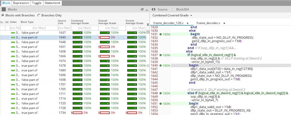
The capability to see combined results in vManager Verification Management is a powerful feature of the Cadence tool flow and ensures an efficient and thorough verification solution. It enables verification signoff using the combined strengths of different verification techniques.
ECC for PCIe 6.0
Primary Function
The error correction code (ECC) block contained an encoder for the transmit direction and decoder for the receive path. It corrects up to three byte burst errors per 256-byte frame.
Verification Challenge
The challenge is to fully verify all correctable burst error byte patterns within a frame, including the multiple ways of corrupting individual bytes.
Benefits and Efficiency of Formal
The formal verification work was done in two steps:
Step 1 - The JasperGold sequential equivalence checking (SEC) app compared the Cadence encoder with the example encoder code provided in the PCIe 6.0 specification. The setup connected the inputs of both blocks together and then used a single assertion to check that the outputs of both blocks always match. This gave rapid confidence that our functionality aligned with the golden spec example.
Step 2 - Connect the encoder with the decoder. The JasperGold platform injected byte errors (controlled via constraints) on the output data from the encoder before the errored data was input to the decoder.
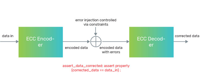
Simple assertions check that data out of the decoder is corrected by comparing it with the input data to the encoder. The environment was fast to build, taking around a day to create the initial version and to find the first bugs. The bugs were corner cases that could have taken a huge number of simulation cycles to catch and demonstrated the efficiency of this formal setup. Note that both setups required some over-constraining of the 256-byte frame data to achieve full assertion passes. Unconstrained versions of the frame data were also run for days on long bug hunting regressions and, as expected, returned explored rather than full passes. These explored results are still valuable and give further confidence in the design.
CXL Arb/Mux
Primary Function
The CXL Arb/Mux exists between the physical and link layers of the Cadence High-Performance Controller for CXL 2.0 and provides dynamic multiplexing of data and control information destined for the CXL.io and CXL.cache/CXL.mem link layers. The transmitting Arb/Mux includes an arbiter that grants requests from the different CXL link layers in addition to creating 544-bit flits that include the 512-bit data plus a 16-bit protocol identifier and a 16-bit CRC. These 544-bit flits are subsequently passed to the physical layer in 512-bit data beats. In the receive direction, inbound CXL flits are unpacked—the protocol identifier and CRC are stripped—and the associated protocol identifier determines to which CXL link layer the data is forwarded. Each CXL link layer has a virtual link state machine (vLSM) that manages power state transition requests. Its main functions are
- Resolving each vLSM state to a single physical layer request
- Generating and receiving Arb/Mux link management Packets (ALMPs) to synchronize power-state transitions across the link between each of the link layers
Each vLSM is responsible for its power state. Local link layer requests or requests from the remote vLSM indicate transitioning states based on these requests.
While the CXL v2.0 specification describes the Arb/Mux vLSM as a hardware-finite state machine, in reality, it is more complicated: The digital architecture of the vLSM is almost like a software-state machine that is capable of generating and processing ALMP while responding to power state requests from its link layer. As a result, the vLSM architecture must be able to correctly handle the order of priority and race conditions which occur due to the asynchronous nature of ALMP and CXL link layer inputs. Formal was excellent at highlighting all these situations.
Verification Challenge
Significant changes to the Arb/Mux chapter took place between version 1.1 and 2.0 of the CXL specification, with a number of areas of the ArbMux chapter open to interpretation as the specification evolved. Multiple technical sessions were therefore required between the Cadence Arb/Mux design team and the Cadence Arb/Mux formal verification team in parallel to the team attending working group sessions at the CXL Consortium.
Verification Strategy
Two strategies were followed in the Arb/Mux vLSM module formal verification. These strategies enabled technical discussions on a number of grey areas in the specifications.
Strategy 1
For each feature, both positive and negative aspects are analyzed. For example, the CXL specification states:
“When an Active Request ALMP has been sent, receipt of any ALMP other than an Active Status ALMP or an Active Request ALMP is considered an unexpected ALMP and will trigger recovery.”
The all-round analysis has forced us to ask the following questions and to develop additional checks for this feature:
- What happens if active status ALMP is sent without any request?
- What happens if active status ALMP is received without any request?
In general, let us consider a signal “x” and a packet “y”:
- “x” should be asserted or “y” should be sent for “p” number of reasons
- “x” should not be asserted or “y” should not be sent for “n” number of reasons
Where “p” refers to positive checks and transforms to “p” number of assertions, and where “n” refers to negative checks and transforms to “n” number of assertions.
The formal environment auxiliary (AUX) code is written to identify “p” reasons and used to disable “n” assertions.
Strategy 2
In general, for cause-effect feature checks, inputs trigger an assertion to check an expected output. There is, however, a disadvantage in having only this check. For example, what happens if there is an effect without any cause? In order to ensure there are no unexpected changes in outputs or state transitions, each “cause and effect” type check has an accompanying “when there’s an effect, check there was a valid cause”. For example, “when active request ALMP is received in low-power state, DUT goes to retrain state”.
There are two kind of checks applied for this condition in order to make the verification foolproof:
- Assertion 1 (cause-effect check)
- Pre-condition: DUT receiving Active Request ALMP in low-power state
- Check: DUT should reach retrain state
-
- Assertion 2 (effect without cause check)
- Pre-condition: DUT transitioning to retrain state from low-power state
- Check: DUT should have received an Active Request ALMP
-
Note: AUX code support would be required for “Assertion 2”
Once such checks were implemented, the formal team found bugs from “negative” and “effect without cause” checks. These techniques paved the way to highlight the grey areas in the standard specification as well as in the design implementation specification.
Formal Benefits
The controller team analyzed in detail the following example grey areas as a result of the formal environment—What happens if the DUT encounters any of these circumstances?
- Receives valid ALMPs in the wrong state
- Receives valid ALMP but not applicable to a particular mode
- Receives back to back request ALMPs or status ALMPs—redundant
- Receives multiple requests at the same time across different interfaces
- Receives ALMP with reserved values in valid field or non-zero values in reserved fields
These questions and checks paved the way to have deterministic and consistent behavior of the RTL-DUT for noisy inputs and hence making the product robust.
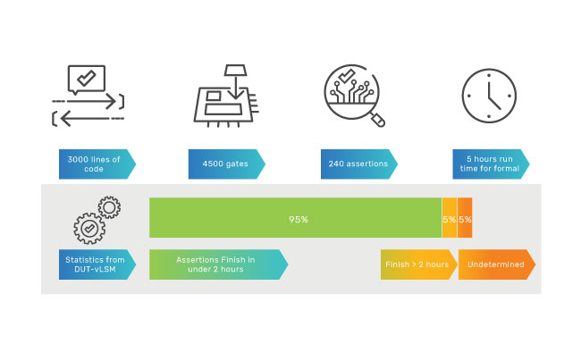
Deploying an independent formal verification engineer to formally verify the Arb/Mux block of the CXL Controller identified several areas of the CXL specification that required clarification. At Cadence, these Arb/Mux discussions took place within a small group of engineers, namely the block designer, the formal engineer, the technical lead, and the CXL IP architect. The controllability and quick turnaround time at the Arb/Mux formal level allowed for rapid development and improvement of the Arb/Mux IP block, while the complex UVM top-level testbench was developed in parallel. Figure 7 summarizes some key statistics from this exercise.
Summary
Assertion-based formal verification continues to demonstrate value in the development of leading-edge standards, across the Cadence Controller portfolio for PCIe. Although formal verification using the Cadence JasperGold platform has been used in a targeted way, it has proven to be a key tool for solving very complex verification challenges and maximizing overall verification efficiency.
- Approximately 10% of the total bugs found during PCIe and CXL verification were via formal verification
- The engineering effort to find this 10% of project bugs required significantly less than 10% of the project’s verification team, therefore demonstrating a high return on investment
- The bugs found by formal verification were mainly non-trivial as most of the blocks had undergone some initial verification using a UVM testbench
- The formal work also led to significant improvements in internal documentation where specification gaps and ambiguities were quickly identified and cleaned up
- The formal work led to significant reductions in the top-level simulation effort: The improved block quality reduced the time spent debugging failing simulations, while closing coverage at the block level prevented the need to repeat full metric closure of these same blocks in simulation
The adoption of formal verification for critical sub-modules of the IP is particularly important in newly released standards where the specification is raw and prone to different reader interpretations, coupled with the fact that the independently developed VIP is being developed in parallel to the Design IP and will take time to reach maturity for top-level testing.
Further Resources
- Cadence Design IP Portfolio: IP
- Paul McClellan, “CCIX Update: TSMC, Xilinx, Cadence, Arm...and Jasper”, Breakfast Bytes blog, posted November 28, 2017
- Cadence, “Arm, Cadence and Xilinx Introduce First Arm Neoverse System Development Platform for Next-Generation Cloud-to-Edge Infrastructure, Implemented on TSMC 7nm Process Technology,“ press release, announced March 12, 2019